

System for manufacturing a pinhole-free Hole Transport Layer (HTL) compatible with perovskite-based devices (No. 0076, 0087)
|
|
|
<< Back to all technologies |

Summary
A novel system for manufacturing a defect-free HTL used in perovskite solar cells or other semiconductor devices.
The global perovskite market size is over 450 million USD and is expected to grow at a CAGR of 30.8%. Perovskites are at the forefront of materials research because of their wide range of potential applications including solar cells, LED lights, display screens, memory devices (RAM), lasers, batteries and photodetectors. Hole transport layer (HTL) materials, a critical component of hole transport in perovskite devices, exert a tremendous impact on the power conversion efficiency and stability. However, due to pinhole defects in HTLs, it has been difficult to obtain stable power efficiency (<360 hours in air). Furthermore, existing HTL manufacturing techniques are not robust enough for fabricating perovskite-based devices with doped layers, multi-junction or tandem cell structure, heterostructure construction, or other advanced optoelectronic structures. Here, we present a promising system developed by a group of researchers led by Prof. Yabing Qi. The developed system significantly reduces the amount of pinhole defects in the HTL and thus improves the performance of energy transport of perovskites.

Applications
- Solar Cell
- Batteries
- Semiconductor Devices (LED, memory, photodetector)
Advantages
- Reduced pinhole defects
- Higher power efficiency stability (840 hours in air)
- Compatible with complex semiconductor construction
Click on the images to enlarge
Technology
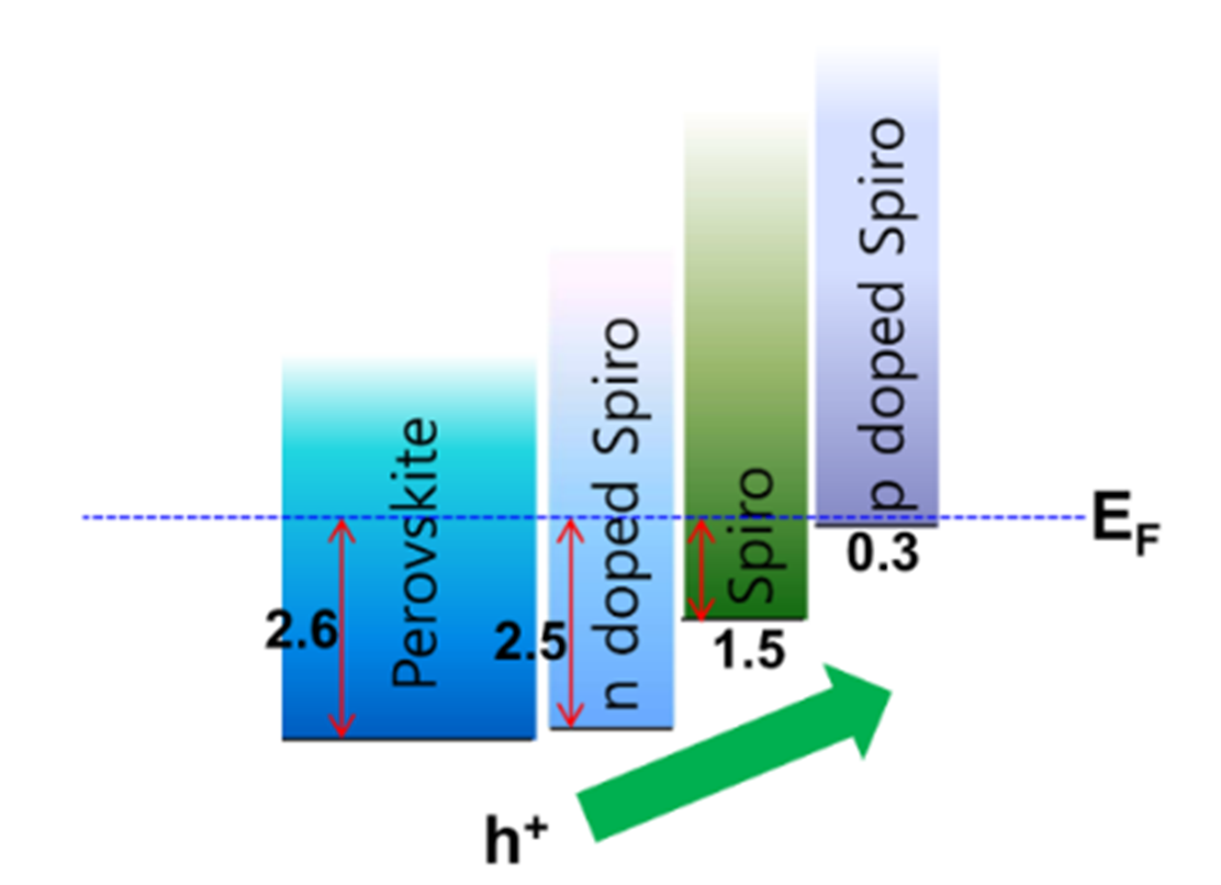
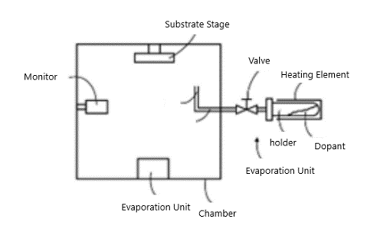
The technology is based on a system for fabricating a stable and defect-free HTL. Firstly, a perovskite layer is formed. Then, by vacuum evaporation, an HTL is formed on the perovskite layer. The HTL includes three sublayers formed by evaporation, (1) an n-doped hole transport material (HTM); (2) an undoped HTM; (3) and a p-doped HTM.
Media Coverage and Presentations
CONTACT FOR MORE INFORMATION
![]() Graham Garner
Graham Garner
Technology Licensing Section
![]() tls@oist.jp
tls@oist.jp
![]() +81(0)98-966-8937
+81(0)98-966-8937