

Chemical Vapor Deposition (CVD) System for Manufacturing Lead-Free Perovskite (No. 0059, 0064, 0092)
|
|
|
<< Back to all technologies |

Summary
A novel CVD system for manufacturing lead-free perovskite layers used in solar cells or other semiconductor devices.
The global perovskite market size is over 450 million USD and is expected to grow at a CAGR of 30.8%. Perovskites are at the forefront of materials research because of their wide range of potential applications including solar cells, LED lights, display screens, memory devices (RAM), lasers, batteries, and photodetectors. However, current CVD systems use lead which is environmentally unfriendly. Here, we present a promising perovskite manufacturing system developed by a group of researchers led by Prof. Yabing Qi. The developed CVD system produces a lead-free perovskite-based product.

Applications
- Solar Cell
- Batteries
- Semiconductor Devices (LED, memory, photodetector)
Advantages
- Lead-Free
- Planar Structure
- Minimized Air-Induced Oxidation
Click on the images to enlarge
Technology
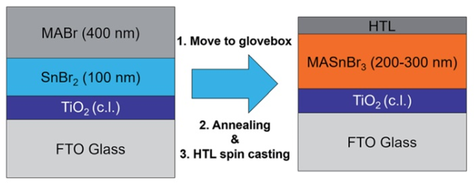
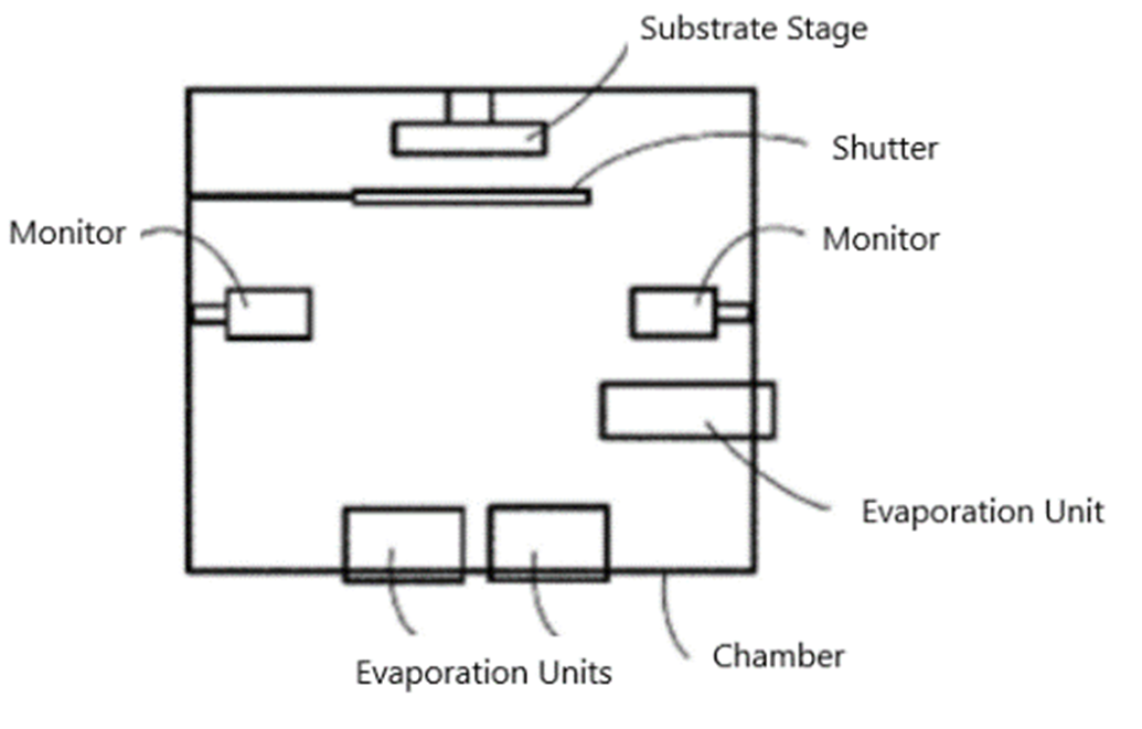
The technology is based on a novel CVD system for fabricating a lead-free perovskite film. The system is based on vacuum evaporation. Firstly, an Sn halide material is deposited on a substrate to form a first layer. Next, an organic halide material is deposited to form a second layer on the first layer. Finally, the sequentially deposited two-layer film substrate is annealed. During the annealing, the materials of the two layers inter-diffuse and react to form the lead-free perovskite film. Essentially, the organic halide layer is formed to cover and protect the Sn halide from air-induced oxidation. A device including the lead-free perovskite film formed by using this system exhibits good stability.
Media Coverage and Presentations
CONTACT FOR MORE INFORMATION
![]() Graham Garner
Graham Garner
Technology Licensing Section
![]() tls@oist.jp
tls@oist.jp
![]() +81(0)98-966-8937
+81(0)98-966-8937