

Microscopy Research
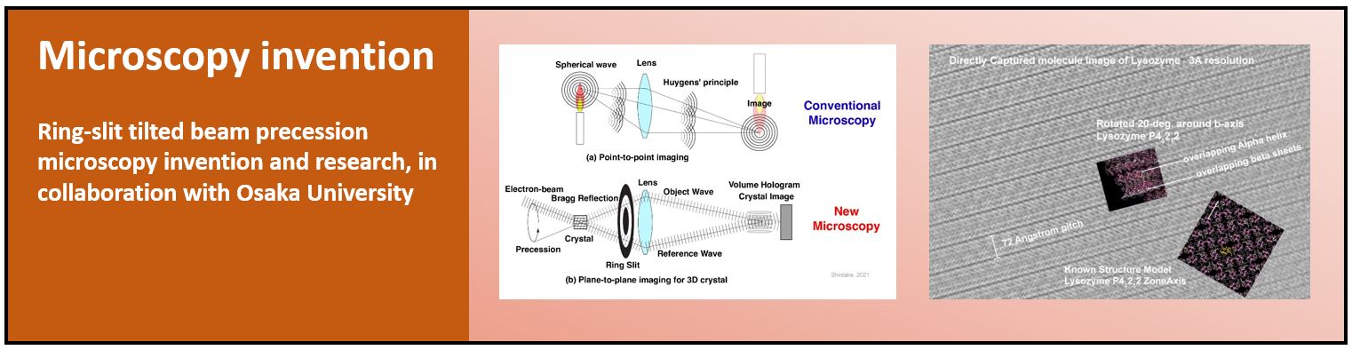
We successfully captured a high-resolution image of molecule array inside protein crystal by our new electron microscopy based on OIST invention (https://arxiv.org/abs/2105.03850). It was believed impossible to see inside the protein crystal at atomic resolution before.
In the conventional optics (upper figure), the light wave emitted from a point source in the candle propagates through lens and focus into a point at downstream. This is point-to-point imaging system. Optical and electron microscopes are same in this concept. On the other hand, our new microscope (lower figure) works as plane-to-plane imaging. The reflected wave from the crystal goes through the ring slit and focus at downstream and overlap with illumination beam, create interference fringes. Quantum mechanical probability function tells us the electron wave takes maximum on the lattice plane inside the crystal, which is imaged on the detector. What we get on the detector is 2D projection image of the crystal. Because of the ring slit, the spherical aberration of the focusing lens inside the electron microscope is effectively eliminated, and thus it may reach atomic resolution. There will be many applications, in biology, in material science, or molecule-based technology development.
"Development of Low Energy Holography Electron Microscope."
Tsumoru Shintake, Hidehito Adaniya, Masao Yamashita, Martin Philip Cheung.
KENBIKYO - The Japanese Society of Microscopy (2017) 52: 51-54.
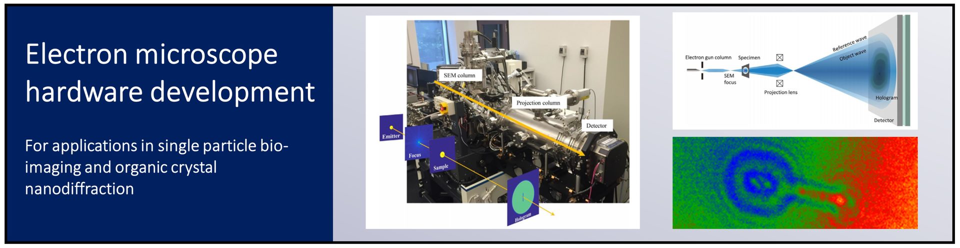
"Development of a SEM-based low-energy in-line electron holography microscope for individual particle imaging".
Hidehito Adaniya, Martin Cheung, Cathal Cassidy, Masao Yamashita, Tsumoru Shintake.
Ultramicroscopy (2018) 188:31-40. doi: 10.1016/j.ultramic.2018.03.002.
Prof. Dennis Gabor invented holography in the 1940’s. His original purpose was to the cure spherical aberration problems in electron microscopes. However, due to technical problems like insufficient beam quality, his original idea was not realized. After the invention of optical lasers in the 1960’s, holography was realized and widely utilized for three-dimensional image recording, high-precision geometrical measurement, and compressed data recording. Prof. Dennis Gabor was awarded the Nobel Prize in Physics in 1971 "for his invention and development of the holographic method”.
In our research, we take up the challenge of realizing his original idea using today’s advanced electron microscopy technology and numerical data analyzing capability.
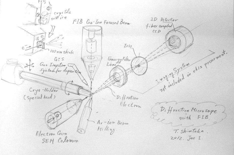
Our equipment uses a high-performance SEM column as a coherent electron source. We place a cryo-sample on a rotatable stage at target position. First, we inspect the sample in SEM mode, then we cut the sample into thin membranes using FIB: Focused Ion Beam tool. We then put the electron beam on the membrane sample and take a diffraction from downstream using a two-dimensional electron detector. Using numerical processing, the electron phase is recovered, and the real image is reconstructed through back-Fourier transformation.
This microscopy will be applicable to the following the research areas in bio-science, physics and technology.
(1) DNA and virus imaging, (2) Protein structure determination using two-dimensional protein crystals, (3) Membrane protein analysis using micron-sized crystals, (4) Ice embedded single bio-particle imaging, (5) Carbon nanotube, fullerene and various kinds of nano-particles.
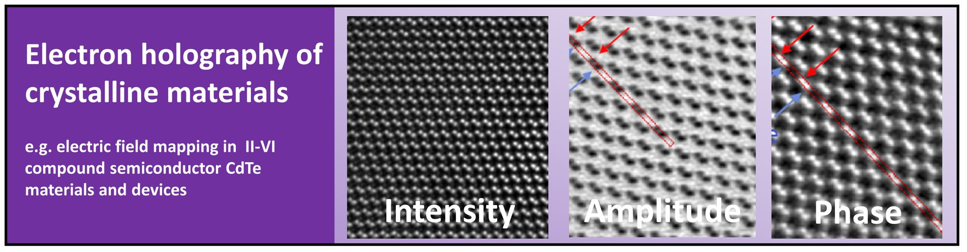
Off-axis electron holography allows quantitative measurement of the amplitude and phase of the electron wave which passes through a specimen, to atomic resolution. Measurement of electron wave phase in turn enables quantitative mapping of electric and magnetic fields in the specimen. This is of particular relevance for semiconductor devices, where atomic scale structures and defects can have a macroscopic effect on the electrical performance of the device.
In this project, as a target material we focus on the detector-grade single crystal CdTe and devices. CdTe has been used for many years in niche gamma-ray astronomy applications, but today is also attracting a lot of attention for mainstream medical imaging technology. We collaborate with a global leading manufacturer of CdTe detector devices (Acrorad Ltd), who are located close to OIST in Okinawa prefecture.
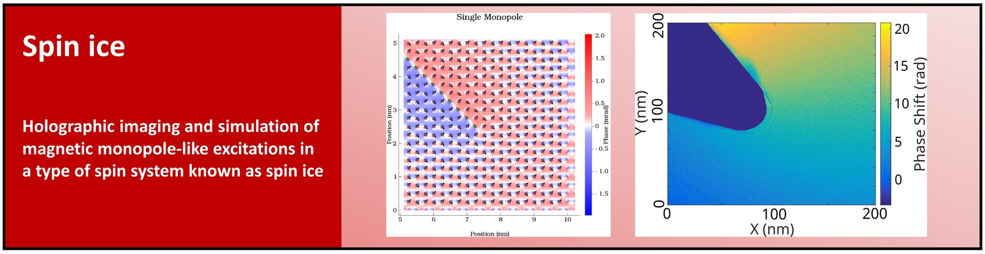
Electron holography is a popular microscopy technique that allows for the visualization of electromagnetic fields within and without of materials. It has made possible the detection of many unique phenomena, such as the Aharonov-Bohm effect and magnetic skyrmions. We are working on designing electron holography experiments to image magnetic monopole-like excitations in a type of spin system known as spin ice. These monopole analogs have been indirectly detected, but holography presents a good chance to image them directly. To realize this experiment, we are taking measurements of larger scale approximations of spin ice monopoles made from single domain magnetic structures, as well as simulating the spin ice experiment with finite element methods. All of this work comes together to build understanding of the technical requirements that will ultimately be necessary to observe monopoles in spin ice directly.