FY2018 Annual Report
Quantum Wave Microscopy
Professor Tsumoru Shintake
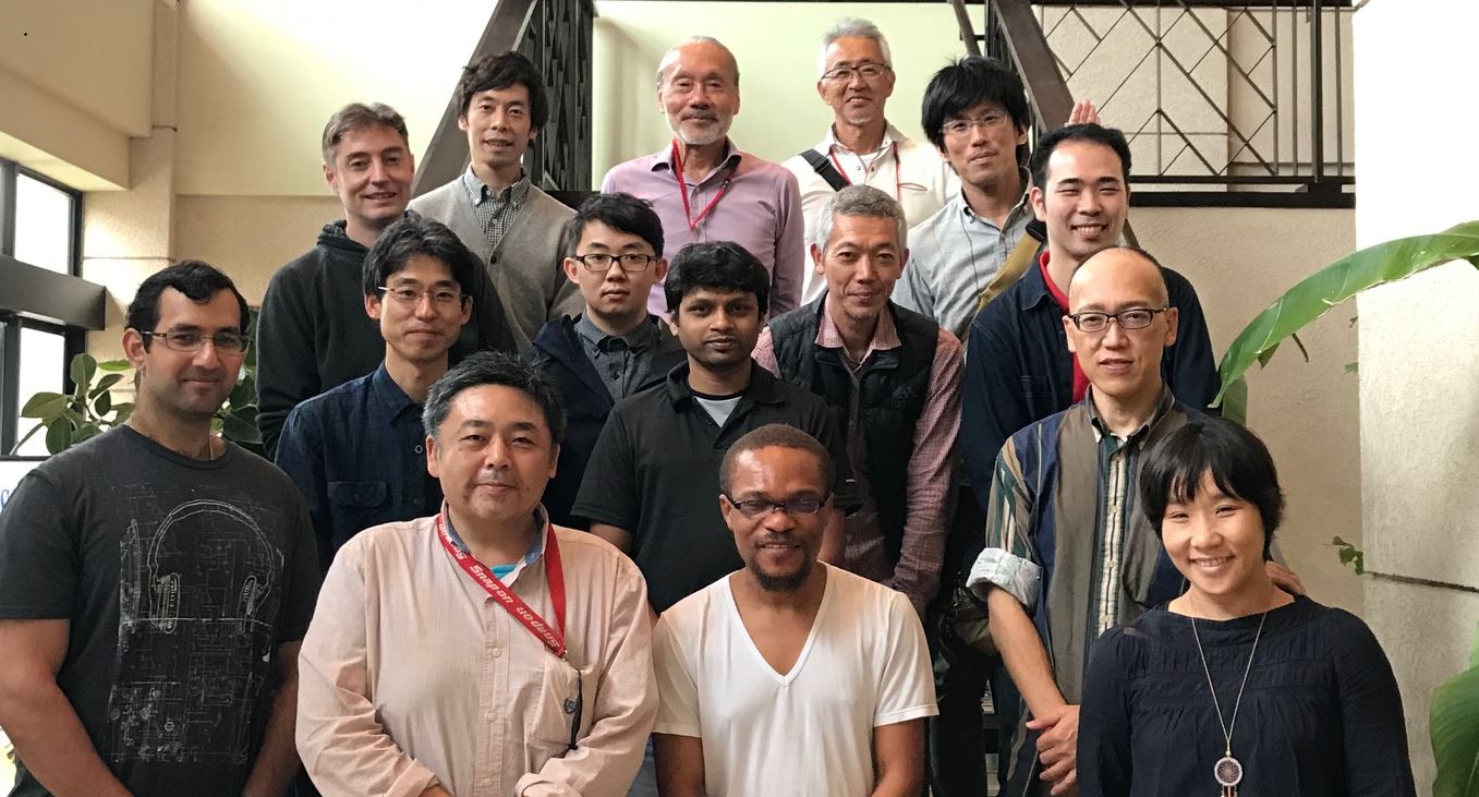
Back row, L to R: Martin Cheung, Prof. Tsumoru Shintake, Hideki Takebe, Katsutoshi Shirasawa
Middle row: Cathal Cassidy, Masao Yamashita, Jun Yamamoto (visiting intern), Paresh Halder, Shuji Misumi, Makoto Ginya, Hidehito Adaniya
Front row: Ankur Dhar, Jun Fujita, Chola Kalale, Yoko Shintani
(Missing from photo: Ryusuke Kuwahara, Seita Taba)
Abstract
1. Electron microscope research continued with a number of projects, with a central theme of applying electron holographic methods for phase contrast imaging of organic and materials specimens.
The projects cover the range of disciplines needed for successful electron microscopy, namely: i) hardware development and optimization ii) specimen preparation and optimization, iii) experimental data acquisition, iv) data analaysis and reconstruction.
The projects and responsible team members are included below:
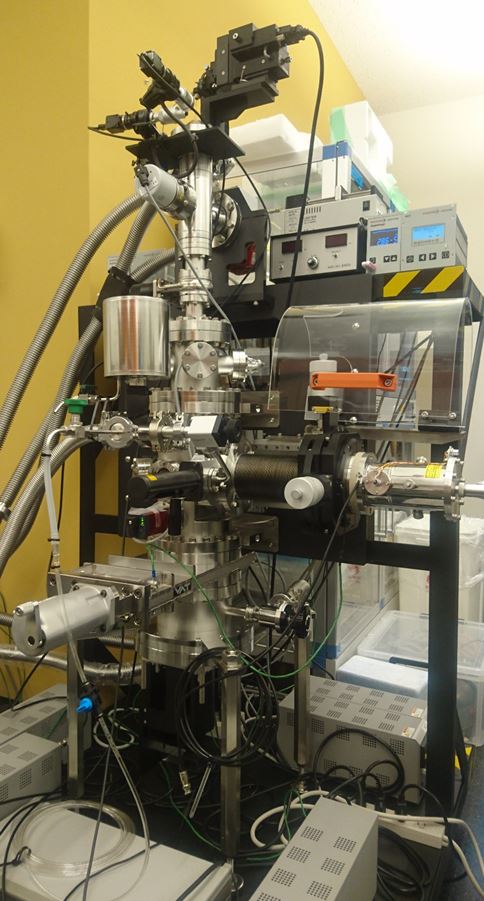
- Development of a dedicated low kV holography electron microscope (Dr. Hidehito Adaniya)
- Development of an electrospray deposition system (EMDS) for dispersing organic specimens onto grids for cryoEM observation (Dr. Masao Yamashita)
- Utilization of graphene and its derivatives to improve specimen preparation for cryoEM (Dr. Martin Cheung)
- Single particle cryoEM of organic specimens (Dr. Ryusuke Kuwahara)
- Electron holography for imaging of electric field distributions in semiconductor devices (Dr. Cathal Cassidy)
- Electron holography for imaging of magnetic field distributions in magnetic spin ice (Mr. Ankur Dhar, PhD student)
- Exploration of novel application of electron holography and electron diffraction for organic microcrystal structure determination (Prof. Shintake, with all team members)
2. Ocean energy
In FY2018, we started hardware development of waterproof electric generator and robust open-water turbines. We successfully demonstrated the stability of the freestanding turbine in the breaking wave, and generation of electricity in the Maldives in FY2018. Further details are included below.
1. Staff
- Dr. Katsutoshi Shirasawa, Staff Scientist (until March 2019)
- Dr. Cathal Cassidy, Staff Scientist
- Dr. Ryusuke Kuwahara, Staff Scientist
- Dr. Hidehito Adaniya, Postdoctoral Scholar
- Dr. Masao Yamashita, Staff Scientist
- Dr. Martin Philip Cheung, Postdoctoral Scholar
- Dr. Paresh Halder, Postdoctoral Scholar
- Dr. Makoto Ginya, Postdoctoral Scholar
- Hideki Takebe, Specialist
- Jun Fujita, Technician
- Shuji Misumi, Technician
- Chola Kalale, OIST PhD Student (until March 2019 - PhD successfully completed)
- Ankur Dhar, OIST PhD Student
2. Collaborations
2.1 Theme: Development of artificial spin ice samples for electron holography studies
- Type of collaboration: Joint research
- Researchers:
- Mr. Ankur Dhar, student, OIST
- Professor Jun Mizuno, Waseda University
- Mr. Hiroyuki Kuwae, student, Waseda University
2.2 Theme: Comparison of low energy microscopy techniques
- Description: AT OIST, we have developed specific competence in preparing low-kV compatible ice-embedded samples. We are collaborating with Hitachi to understand how such samples appear in high-end commercial microscopes, and how the performance compares with our self-developed holography microscope.
- Type of collaboration: Joint research
- Researchers:
- HITACHI
- Dr. Hidehito Adaniya, Dr. Martin Cheung (OIST)
2.3 Theme: Electron holography & diffraction for nanocrystal structure determination
- Description: At OIST, we are performing holography and diffraction experiments, while Dr. Latychevskaia is providing support for simulation and analysis of the experimental data.
- Type of collaboration: Joint research
- Researchers:
- Dr. Cathal Cassidy (OIST)
- Dr. Tatiana Latychevskaia, (Paul Scherrer Institute & University of Zurich, Switzerland)
2.4 Theme: Electron holography studies of CdTe gamma-ray sensor devices
- Description: At OIST, we are performing holography experiments on CdTe. The group at University of Tokyo have long experience in building functional devices from CdTe, and are providing advice on junction and defect properties within such devices.
- Type of collaboration: Joint research
- Researchers:
- Dr. Cathal Cassidy (OIST)
- Prof. Shin'ichiro Takeda (Kavli Institute, University of Tokyo)
- Prof. Tadayuki Takahashi (Kavli Institute, University of Tokyo)
2.5 Theme: Structural and functional studies of virulence factors from clinically significant bacterial pathogens (AMED)
- Description: Collaborating closely with members of the Agency for Medical Research and Development (AMED) scheme at OIST, this project seeks to utilise high-resolution cryo-electron microscopy to study isolated virulence factors from clinically significant bacterial pathogens, such as Shigella, Salmonella and Yersinia. This project will potentially have important implications for new antibacterial and vaccine development.
- Type of collaboration: Collaborative project with the Agency for Medical Research and Development (AMED) scheme at OIST
- Researchers:
- Dr. Martin Cheung, Mr. Seita Taba (QWM unit, OIST)
- Dr. Ryo Kanno, Dr. Malgorzata Hall (AMED)
- Dr. Bruno Humbel (AMED)
3. Activities and Findings
3.1 Electron microscope group
3.1.a Microscope hardware development (Dr. Hidehito Adaniya)
This year, we have successfully obtained first holographic images of ice-embedded viral specimens in low energy domain (20kV). This success is due mainly to specially optimized electron optics and to specially prepared cryo-sample optimized to low energy domain. (see 3.1.b)
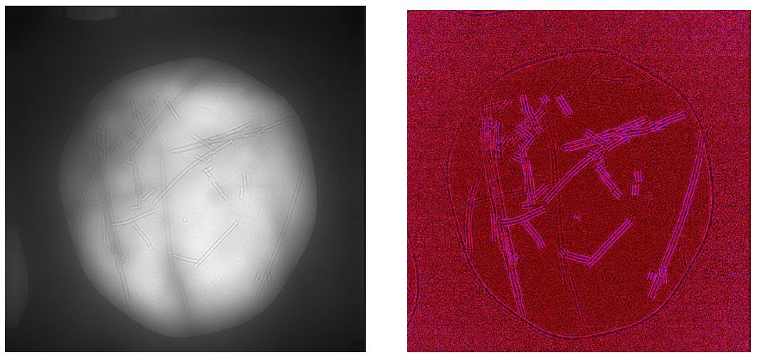
Figure 1 Reconstructed holographic images. Left: Amplitude reconstruction of ice-embedded of TMV specimen, Right: Phase reconstruction
Additionally, we have compared the quality of holographic images with the following modification in the electron beam column; 1) by comparing the two different emitters, Schottky emitters and Cold Field Emitter, which are expected to generate different degree of coherence in electron beam, and 2) by comparing the two beam apertures with different diameter size, few tens of micrometer to few hundred micrometers, which are expected to generate different diffraction limit which is expected to affect the final resolution of the images.
We have also collaborated with HITACHI, to make a comparison between incoherent imaging and coherent imaging in the low energy domain by using conventional STEM and our holographic microscope (DMF). This work is also underpinned by our advances in specimen preparation for low-kV ice-embedded samples (see 3.1.b). We worked with HITACHI for high resolution STEM imaging, using SU9000, capable of both BF and ADF imaging with few hundred mrad ADF acceptance angle. Due to the difference of the characteristics of 1) STEM imaging, making use of both elastically and inelastically scattered electrons at the specimen, and of 2) Holographic imaging, making use of mostly elastically scattered electrons for image formation. It is very informative to investigate both imaging approaches for further development of our microscope.
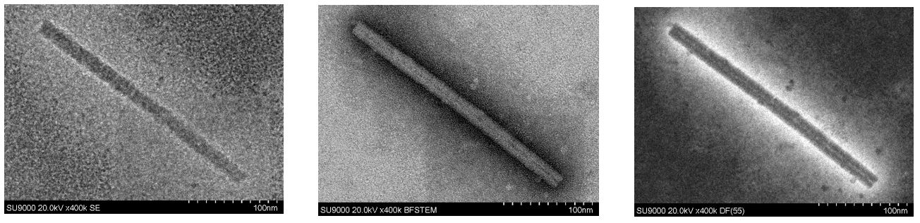
Figure 2 Left: SE image of stained TMV at 20kV, Middle: Bright field image, Right: Annual dark field image
3.1.b EMDS development (Dr. Masao Yamashita)
The low energy TEM imaging necessitates exceptionally clean (i.e. free from background contamination) specimen for the best possible image quality. Starting from 2016 we started developing a new vacuum hardware that allows in vacuo preparation of the specimens on an "ultraclean" graphene support film. The basic construction and installation of the hardware has been completed in 2017 (see the image). We are now performing an extensive study on the applicability of the system to a range of samples including biological macromolecules. Concurrently, the hardware is continuously updated for the better performance.
3.1.c Graphene and derivatives for cryoEM preparation (Dr. Martin Cheung)
Part of our research concerns the development of cost-effective, easily adoptable alternatives to currently available sample preparation regimes, especially through the use of atomically thin materials such as graphene and graphene oxide. Our innovative methods have found application in cryo-TEM and low-energy electron holography.
Working with low-kV electron beams forces stringent requirements on ice thickness and quality for cryoEM. This year, we demonstrated a clear and repeatable improvement in specimen dispersion in ultrathin vitreous ice with our customized recipe for utilizing graphene oxide as part of the vitreous ice specimen preparation procoess. This work resulted in a publication in the Journal of Structural Biology (reference below).
3.1.d Electron holography studies of CdTe (Dr. Cathal Cassidy)
The year began with the good news that our Kakenhi application for electron holography studies on CdTe was successful. This proposal outlined four stages over 3 years: i) CdTe electron transparent lamella optimization, ii) calculations, modeling and simulations of electron wave propagation through single crystal CdTe, iii) Experimental optimization of spatial and voltage resolution, iv) quantitative mapping of nanoscale electric fields at CdTe device junctions and defects.
In line with planning, work this year has focused on stage 1 - optimization of CdTe electron transparent lamella preparation. We worked on optimizing Focused Ion Beam Milling of CdTe, developed a methodology for performing cryo-FIB milling of this delicate semiconductor (Fig. 1a), and performed in situ and ex situ processing of the lamella surface to control surface oxidation and contamination (Fig. 1b).
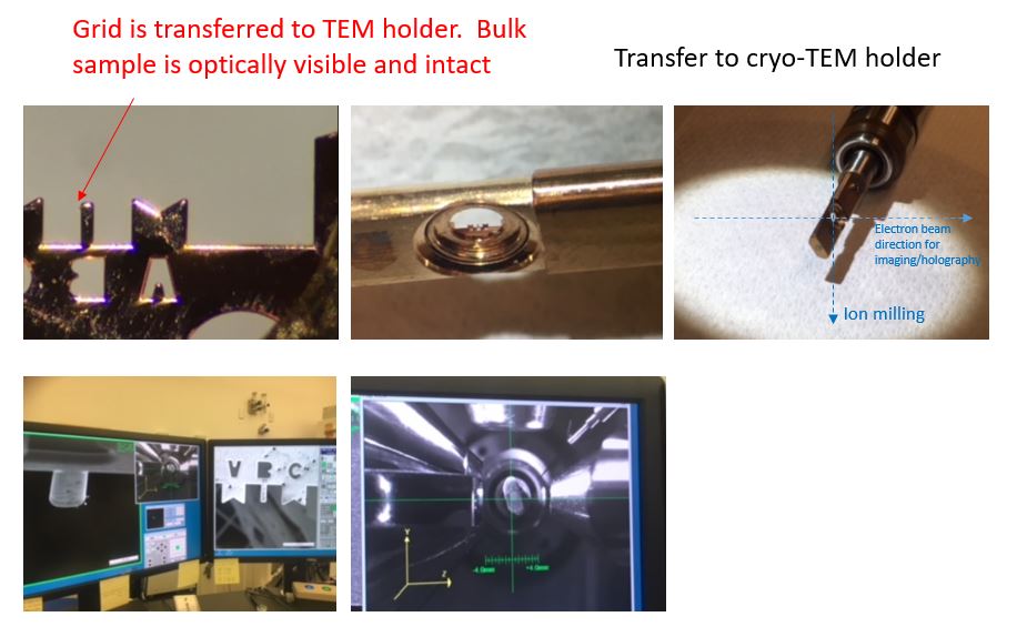
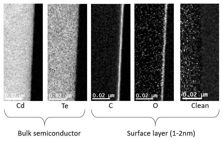
Fig. 1 - Lamella optimization (a) Development of in-house method for performing cryo-FIB on semiconductor specimens (b) Electron Energy Loss Spectroscopy (EELS) maps of the surface condition of CdTe as a function of different surface treatments.
Overall, we made significant progress. The improvement in specimen quality can clearly be seen in the HRTEM images below (Fig. 2), with earlier lamellae on the left and recent lamellae on the right.
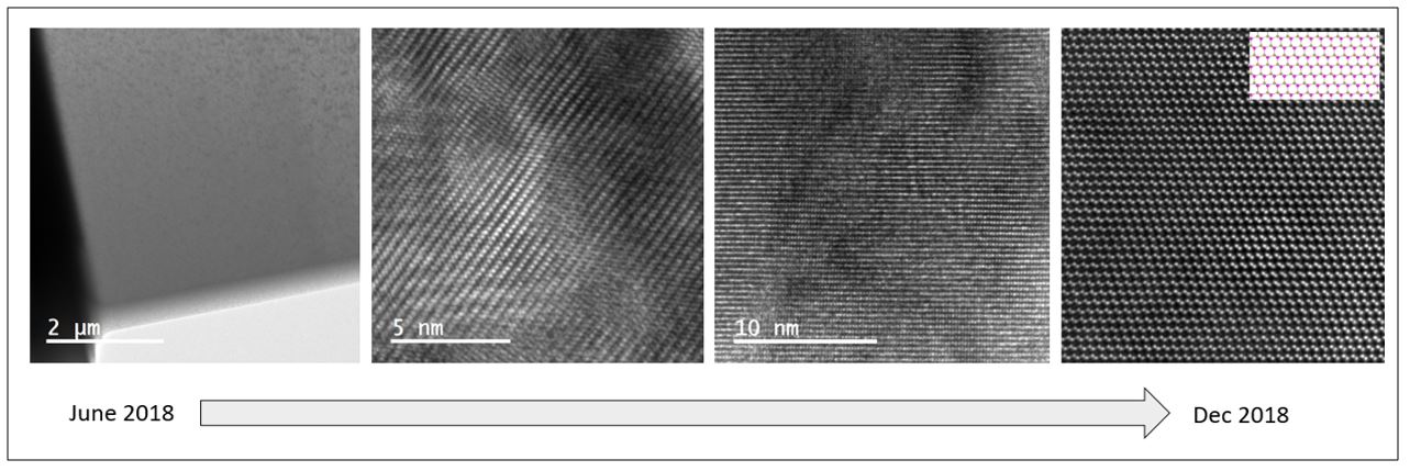
Fig. 2 - Illustration of the improvement in CdTe electron transparent lamella quality during 2018.
We successfully obtained conventional TEM images of CdTe (Fig. 3 below, with false colour) which are comparable with the state-of-the-art. These images are unremarkable in the sense that such sub-Angstrom resolution is typical from modern microscopes. The images do, however, serve to confirm that the electron-transparent lamellae preparation process is well optimized.
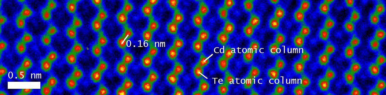
Fig. 3 - High resolution conventional TEM image of <110> oriented CdTe single crystal. The characteristic dumbbells, with spacing of 0.16nm, can easily be resolved.
Furthermore, aside from conventional TEM, we began electron holography trials and obtained atomic resolution holograms, displaying both amplitude and phase distributions (Fig. 4) This is a preliminary but quite exciting result, and experiments and analysis are ongoing.
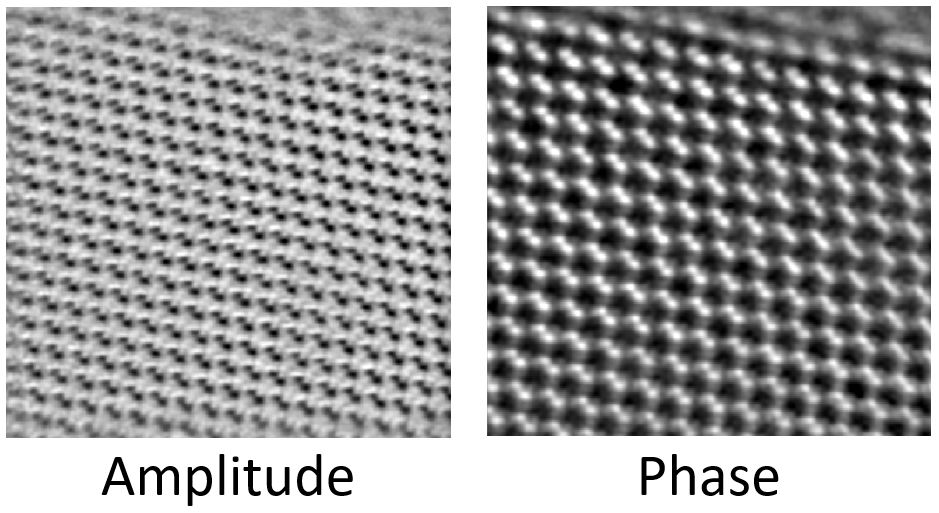
Fig. 4 - Atomic resolution electron hologram acquired from <110> oriented single crystal of CdTe. In contrast to the previous image (Fig. 3), in this case both the ampitude and phase of the electron wave have been individually recorded. This will facilite a range of further quantitative investigations of the electrical potentials associated with the atomic structure itself, as well as dopant species, junctions and crystallographic defects.
We have also begun preliminary work in stage II - calculations and simulations of electron wave propagation through CdTe. An example is illustrated in Fig. 5 below. In this example, we show a multislice simulation of a 300kV electron wave which passed through 2.8nm of CdTe (about 6 atoms in <110> orientation). Efforts are ongoing to optimize the simulation environment, and to compare the output of the simulations to the experimental data (as shown in Fig. 4).
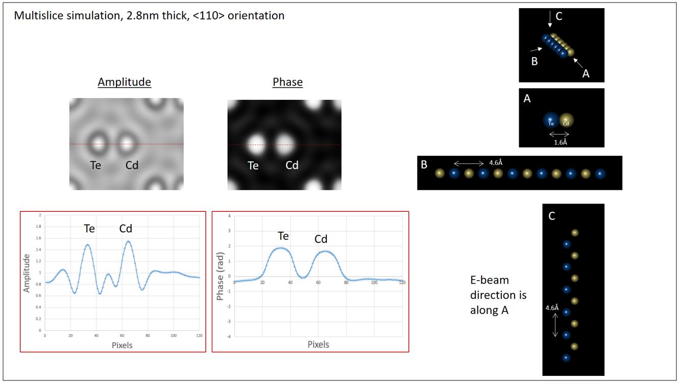
Fig. 5 - Multislice simulations of 300kV electron wave propagation through CdTe. In this case, the specimen is oriented to the <110> zone axis, is approximately 6 atoms thick, with an interatomic spacing of 0.46nm in the z (wave propagation) direction.
At the conclusion of the year, we began contacts with the Takahashi group at the Kavli Institute of the University of Tokyo, to discuss collaborations. The Takahashi group are global leaders in CdTe device development. A first meeting took place from 27-29th January (University of Tokyo), during which Dr. Cassidy presented a seminar at the Kavli Institute. The next meeting is scheduled in Okinawa for 23rd April 2019, and it is hoped that a deep and fruitful partnership can be developed.
3.2 Ocean Power Generation Group
Our Wave Energy Converter (WEC) is based on a new working principle, which uses small size turbine in breaking wave, originally created at OIST in 2014. The hardware R&D, which we now refer to as the OIST Wave Energy Project Phase-I, was started in 2016[1,2]. Two half-scale WECs (35 cm turbine, 1.3 kW peak) were installed at the eastside beach of Kandooma Island in the Maldives in May 2018, and have accumulated over 7,200 hours (ten months) of continuous operation at the time of writing (February 2019). Another two full-scale WECs (60 cm turbine, 8 kW peak) were installed in November 2018, and have accumulated over 2000 hours (three months) of operation. Recently, we have tested 1st prototype model of Ducted-WEC (taper waveguide and ducted turbine), and obtained roughly six times higher power than bare turbine.
In FY2018, we started hardware development of waterproof electric generator and robust open-water turbines. We successfully demonstrated the stability of the freestanding turbine in the breaking wave, and generation of electricity in the Maldives in FY2018.
Further details on wave energy research are included here.
4. Publications
4.1 Journals
- Kotani N, I. Y., Nakano T, Sato I, Kuwahara R, Yamaguchi A, Tomita M, Honke K, Murakoshi T. (2018). "Tumor-dependent secretion of close homolog of L1 results in elevation of its circulating level in mouse model for human lung tumor." Biochem Biophys Res Commun 501(4): 982-987.
- Cheung M, A. H., Cassidy C, Yamashita M, Li KL, Taba S, Shintake T. (2018). "Improved sample dispersion in cryo-EM using "perpetually-hydrated" graphene oxide flakes." Journal of Structural Biology 204(1): 75-79.
- Shintake, T. (2018). New Wave Energy. Clean Energy 27: 14-19.
- Hideki Takebe, K. S., Jun Fujita, Shuji Misumi and Tsumoru Shintake (2018). "Development of OIST Wave Energy Converter Monitoring System for Maldives Island Experiment." Journal of Energy and Power Engineering 12: 375-384.
4.2 Books and other one-time publications
Nothing to report
4.3 Oral and Poster Presentations
- H.Adaniya, M. C., C.Cassidy, M.Yamashita, S.Taba, T. Shintake (2018). OIST R&D for low energy diffraction-holography microscope toward non-destructive single molecule imaging III: Cryo-imaging. Kurume City Plaza, Fukuoka, Japan, The 74th Annual meeting of the Japanese Society of Microscopy.
- Ryusuke Kuwahara, T. S. (2018). Structural Analysis of plant alpha Mannosidase by Cryo Electron Microscopy Kurume City Plaza, Fukuoka, Japan, The 74th Annual Meeting of The Japanese Society of Microscopy.
- Cassidy, T. S. a. C. (2018). Possibility of Improved Phasing Method on Micro-ED, Oviedo, Spain, 31st European Crystallographic Meeting (ECM31).
- Dhar, A. (2018). Simulation of Electron Holography of Pyrochlore Spin Ice. University of California Davis, California, USA, Highly Frustrated Magnetism 2018. and International Conference of Magnetism 2018.
- H.Takebe, K. S., J. Fujita, S. Misumi, T. Shintake (2018). Maldives Experiment on Wave Energy Converter using Horizontal Axis Turbine. Saga University, Japan, Ocean Energy Workshop Symposium (OES2018).
- Hideki Takebe, K. S., Jun Fujita, Shuji Misumi, Tsumoru Shintake (2018). OIST Wave Energy Converter Monitoring System for Maldives Island Experiment. Taiwan University, AWTEC2018.
- Shintake, C. C. a. T. (2018). Possibility of Improved Phasing Method for MicroED - experimental aspects, Oviedo, Spain, ECM31, 31st European Crystallographic Meeting.
- Shintake, T. (2018). On Wave Energy Generators Installation in the Maldives. Industry Club of Japan.
- Shintake, T. (2018). SACLA X-ray Laser based on the normal conducting C-brand Accelerator. Maxwell Auditorium, Madrid, Spain.
- T. Shintake, K. S., J. Fujita, S. Misumi, T. Nagahama, T. Shindou, H. Taggart, H. Takebe (2018). Wave energy experiment at Maldives, Taipei, Taiwan, AWTEC 2018.
5. Intellectual Property Rights and Other Specific Achievements
Nothing to report
6. Meetings and Events
6.1 SPH modeling of fiber orientation in a 3D printing process
- Date: July 12, 2018
- Venue: OIST Campus Seminar Room B503
- Speaker: Professor Phan-Thien Nhan (NUS Mechanical Engineering)
6.2 SPH Modeling of Fluid-Structure Interaction
- Date: July 12, 2018
- Venue: OIST Campus Seminar Room B5031
- Speaker: Dr. Xiangyu Hu (Institute of Aerodynamics and Fluid Mechanics, Technical University of Munich)
7. Other
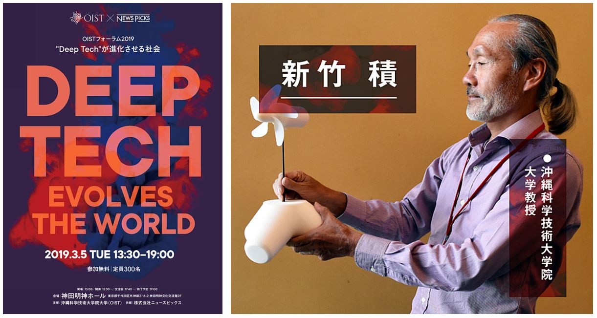
- Prof. Shintake gave a keynote speech at the "Deep Tech evolves the World" forum in Tokyo (Kandamyojin Hall, March 5th 2019).
- Prof. Shintake participated in the OIST outreach program "Science Talk Series Series 2" (Junku do bookstore, Naha, 8th March 2019).