

FY2019 Annual Report
Quantum Wave Microscopy
Professor Tsumoru Shintake
Abstract
Microscopy group
Microscopy and holography research continued on a variety of interdisciplinary projects, building upon the hardware development and sample preparation optimization of previous years. These projects include development of low-kV holography cryo-microscopy, development of an electrospray bio-specimen preparation hardware (EMDS), quantitative microscopy and holography studies of crystalline materials, cryoEM of diverse biological specimens, and exploration of a novel optical microscopy technique.
Wave energy group
The first full-scale Taper-Ducted OIST Wave Energy Converter device was deployed at the Port of Seragaki, Okinawa, on July 2019. The full-scale device started operation on September 2019 and the electricity generated since have been monitored and stored. The device managed to stand against the Typhoon Tapah in September 2019 with minor damage and recorded up to 6kW peak power generation. Two (2) out of 5 turbine blades, unfortunately, failed in January after about 7 months of operation. An observation currently underway to look at the cause of the failure. In addition, 4 more devices are currently being sent to the Maldives.
1. Staff
- Dr. Masao Yamashita, Staff Scientist
- Dr. Cathal Cassidy, Staff Scientist
- Dr. Ryusuke Kuwahara, Staff Scientist
- Dr. Hidehito Adaniya, Research Unit Technician
- Dr. Makoto Ginya, Postdoctoral Scholar
- Dr. Martin Philip Cheung, Research Unit Technician
- Dr. Paresh Halder, Postdoctoral Scholar (until January 2020)
- Dr. Krisna Pawitan, Postdoctoral Scholar (starting July 2019)
- Seita Taba, Research Assistant
- Hideki Takebe, Specialist
- Jun Fujita, Research Unit Technician
- Shuji Misumi, Research Unit Technician
- Ankur Dhar, OIST PhD Student
- Hanley Andrean, OIST PhD Student
- Aditi Pophale, OIST PhD Student (rotation, Fall 2019)
- Gulfiya Kadyrzhanova, OIST PhD Student (rotation, Winter 2020)
2. Collaborations
2.1 Theme: Development of artificial spin ice samples for electron holography studies
- Type of collaboration: Joint research
- Researchers:
- Mr. Ankur Dhar, student, OIST
- Professor Jun Mizuno, Waseda University
- Mr. Hiroyuki Kuwae, student, Waseda University
2.2 Imaging magnetic monopoles in spin ice
- Type of collaboration: Joint research
- Researchers:
- Mr. Ankur Dhar, OIST
- Dr Ludovic Jaubert, CNRS Bordeaux
- Prof. Nic Shannon, OIST
2.3 Theme: Comparison of low energy microscopy techniques
- Description: AT OIST, we have developed specific competence in preparing low-kV compatible ice-embedded samples. We are collaborating with Hitachi to understand how such samples appear in high-end commercial microscopes, and how the performance compares with our self-developed holography microscope.
- Type of collaboration: Joint research
- Researchers:
- HITACHI
- Dr. Hidehito Adaniya, Dr. Martin Cheung (OIST)
2.4 Theme: Electron holography & diffraction for nanocrystal structure determination
- Description: At OIST, we are exploring a hybrid Bragg inline holography/diffraction experimental configuration for nanocrystal diffraction, while Dr. Latychevskaia is providing support for simulation and analysis of the experimental data.
- Type of collaboration: Joint research
- Researchers:
- Dr. Cathal Cassidy (OIST)
- Dr. Tatiana Latychevskaia, (Paul Scherrer Institute & University of Zurich, Switzerland)
2.5 Theme: Electron holography studies of CdTe gamma-ray sensor devices
- Description: We are developing capabilities for quantitative electron microscopy and holography of high resistivity CdTe single crystals and devices.
- Type of collaboration: Joint research
- Researchers:
- Dr. Cathal Cassidy, Dr. Hidehito Adaniya (OIST)
- Prof. Shin'ichiro Takeda, Prof. Tadayuki Takahashi (Kavli Institute, University of Tokyo)
- Prof. Daisuke Morikawa, Mr. Masaki Ageishi (IMRAM, Tohoku University)
- Dr. Hiroto Kasai (Atomic Scale Platform, Hitachi/RIKEN Tonomura microscope)
2.6 Theme: Structural and functional studies of virulence factors from clinically significant bacterial pathogens (AMED)
- Description: Collaborating closely with members of the Agency for Medical Research and Development (AMED) scheme at OIST, this project seeks to utilise high-resolution cryo-electron microscopy to study isolated virulence factors from clinically significant bacterial pathogens, such as Shigella, Salmonella and Yersinia. This project will potentially have important implications for new antibacterial and vaccine development.
- Type of collaboration: Collaborative project with the Agency for Medical Research and Development (AMED) scheme at OIST
- Researchers:
- Dr. Martin Cheung, Mr. Seita Taba (QWM unit, OIST)
- Dr. Ryo Kanno, Dr. Malgorzata Hall (AMED, OIST)
- Dr. Bruno Humbel (AMED, OIST)
3. Activities and Findings
3.1 Electron microscope group
3.1.a Development of electrospray sample deposition system (Dr. Masao Yamashita)
Our unit has been focusing on low voltage holographic imaging of bionanoparticles (such as viruses) using an ultraclean graphene as a specimen support film (Ref. 1). The graphene is logically the best specimen support film for the low voltage TEM/STEM imaging as it is only one-atom-thick and has high electrical conductivity. On the other hand logically the best specimen would be the molecules that are completely free from surrounding solvent molecules. To realize the specimen preparation using such desolvated molecules we have been forcusing on the possibility of using the electrospray ionization method. After 3 years of development, we have built the electrospray molecular deposition device (Fig. 1a and Fig. 1b). The current research focus is to optimize electrospray conditions for various bionanoparticle specimens. Our results so far have demonstrated that highly dehydrated molecular ions such as of large protein complexes and DNA may be produced by the electrospray method without adversely affecting their quaternary structures. Figure 1c is an example image showing a 20 kV secondary electron SEM image of the molecular ion of erythrocruorin protein complex (molecular weight 3.6 MDa) imaged after platinum coating. Our future research is going to focus on establishing a novel vacuum deposition technology using both the graphene support film and the molecular ions generated by the electrospray method.

3.1.b Microscope hardware development (Dr. Hidehito Adaniya & Dr. Martin Cheung)
This year, we have successfully obtained first holographic images of ice-embedded viral specimens, such as TMV, erythrocruorin, and bacteriophage T4, in low energy domain (20kV). This success is due mainly to specially optimized electron optics and to specially prepared cryo-samples, optimized for low energy domain [1-3].
Successful hologram formation in low-energy in-line electron holography is greatly influenced by sample quality. For small biomolecules embedded in vitreous ice films, ice thickness and transparency were found to be decisive factors in successful hologram acquisition and image reconstruction. By combining our graphene oxide-based method with 20 keV in-line electron holographic imaging in DMF4000, we successfully captured low-to-moderate resolution holograms of ice-embedded biomolecules without the need for any form of sample staining or chemical fixation. Images reconstructed by computational back propagation of holograms displayed structural resolution of ~2–3 nm.
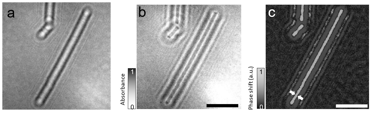 Figure1. In-line electron hologram and reconstructed images of ice-embedded TMV. (a) Hologram at 20kV. (b) Amplitude and (c) phase contrast images of ice-embedded TMV virions were reconstructed separately from an in-line electron hologram captured with an offset of +200 μm from point focus and a total dose of 0.2 e-/Å2. Block arrows indicate edge of reconstructed particle. In both cases, TMV virions display substantial contrast compared with the surrounding ice. All scale bars, 200 nm.main. (see 3.1.x)
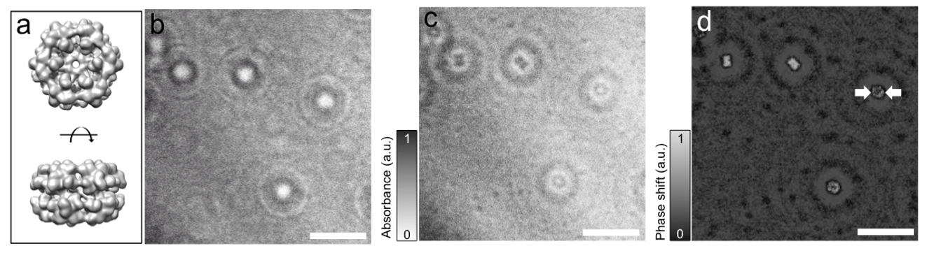 Figure 2. In-line electron hologram and reconstructed images of erythrocruorin. (a) Electron density map of erythrocruorin (PDB: 2627). (b) Hologram of ice-embedded erythrocruorin at 20kV. Reconstructed (c) amplitude and (d) phase contrast images by back propagation. Block arrows in (d) indicate edge of reconstructed particle. A total dose of 0.2 e-/Å2. All scale bars, 100 nm
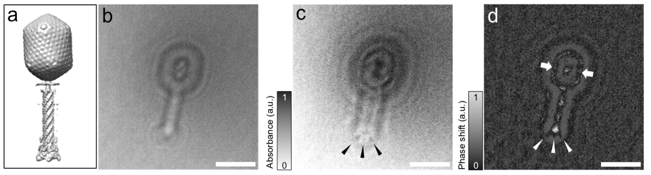
Figure 3. In-line electron hologram and reconstructed images of bacteriophage T4. (a) Electron density map of bacteriophage T4 (PDB: 2774). (b) Hologram of ice-embedded bacteriophage T4 virion at 20kV. Reconstructed (c) amplitude and (d) phase contrast. Arrow heads in (c) and (d) specify clearly discernable tail-spikes. A total dose of 0.2 e-/Å2. All scale bars, 100 nm.
[1] Cheung et al., J. Struct. Biol. (2018) 1: 75-79.
[2] Adaniya et al., Ultramicroscopy (2018) 188:31-40.
[3] Cheung et al., Ultramicroscopy (2020) 209 (2): 112883.
3.1.c Electron holography studies of CdTe crystals and devices (Dr. Cathal Cassidy)
Our primary effort this year has been to understand the physical processes underlying the mean free path (MFP) for electron scattering in CdTe, as measured from electron holography amplitude data. We had previously measured the CdTe mean free path via EELS [Cassidy et al, APL, 2017], but the measured value and underlying physics are rather different for electron holography. Aside from holography, we also employed complementary diffraction and energy-filtering measurements to help deconvolute the various contributions to the observed scattering behaviour. These contributions include hardware specific factors (e.g. aperture collection angles, biprism voltage); as well as more fundamental electronic (e.g. plasmon) and nuclear (e.g. TDS) scattering processes in the specimen. We made good progress this year, and a new manuscript is close to completion.
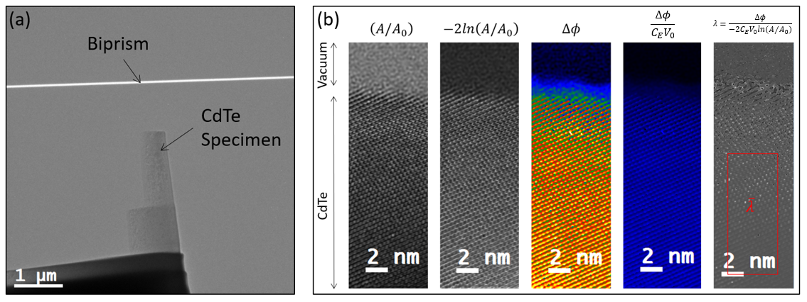
Figure 1. Mean free path for electron scattering in electron holography amplitude measurements. (a) Overview of experimental set-up for off-axis holography, showing thin CdTe lamella and nearby electrostatc biprism (b) Measurements of CdTe-transmitted electron wave amplitude and phase, and associated calculation of mean free path.
In parallel, we continued our efforts to improve specimen preparation for this delicate semiconductor, collaborating with Tohoku University and Hitachi High Technologies. We have spent some efforts to quantify CdTe defectivity as a function of ion milling conditions using a quantitative CBED analysis approach pioneered by Tohoku university. Although this CBED analysis method has been proven to work for silicon [Ageishi et al, JSM75, Nagoya, June 2019], thus far we have been unable to replicate these results in CdTe. CdTe has quite unusual thermomechanical properties, so it is perhaps not surprising that it exhibits diferent behaviour, and we will continue this work to try to understand the underlying mechanisms.
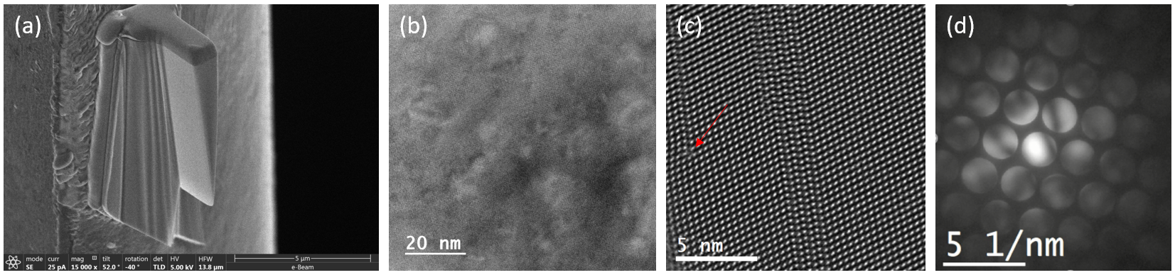
Figure 2. Optimization of specimen preparation, and analysis via quantitiative CBED studies. (a) Wedge specimen prepared at OIST using Focused Ion Beam (b) low magnification image, showing contrast variations associated with lattice damage (c) high magnification TEM images, showing multiple crystallographic faults associated with ion beam milling (d) 300kV energy-filtered CBED pattern from <110> oriented CdTe. We are working with Tohoku University to try to automatically quantify crystal lattice damage as a function of ion beam milling parameters.
In general this year, we spent some effort to network with other labs, gain feedback on our results to date, and form collaborations. Dr. Cassidy attended and presented at a number of workshops, conferences and labs. These included CCEM (McMaster, Canada), ECM32 (Vienna, Austria), JSM75 (Nagoya), OIST-Hitachi Symposium (Tokyo), holography lab at JFCC (Nagoya), and holography lab at the Hitachi Centre for Exploratory Research ("Tonomura microscope", Hatoyama). We have established a number of connections and gained valuable feedback on our work.
An example collaborative relationship established this year is shown below. Via the Atomic Scale Platform, we performed a trial of 1.2MV holography for CdTe using the Tonomura microscope in Hatoyama. As CdTe is a relatively dense, high-Z, opaque material, we were interested to explore the performance of 1.2MV holography when applied to this material. We prepared a wedge specimen at OIST, pre-characterized at 300kV, and then visited the Hatoyama facility for measurement. Example data is shown below (Ack. Dr. T. Akashi, Dr. H. Kasai, Dr. T. Tanigaki (Hitachi) ). This data suggests that useful phase data can be obtained from CdTe specimens up to 1um thick, which is a significant improvement on the 300kV data obtained at OIST, and is important for defect studies in CdTe. Furthermore, we observed that holography fields of view as wide as 7um (squared) can be visualized with dual biprism and custom optical setup.
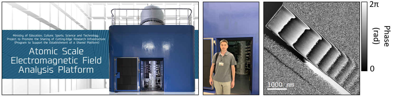
Figure 3. Electron holography on CdTe wedge specimen at 1.2MV. Via the Atomic Scale Electromagnetic Field Analysis Platform, we performed trials using the world leading 1.2MV holography microscope in Hatoyama (developed by the late Prof. Akira Tonomura). This preliminary experiment suggests that, despite the high density and atomic number of CdTe, specimens up to 1um thick can be usefully examined at 1.2MV.
This work is supported by Kakenhi Grant-In-Aid for Scientific Research (#38005, Category - Scientific Research C, “Electron Holography Studies of CdTe”).
3.1.d Electron holography studies of Artificial Spin Ice (Ankur Dhar, PhD student)
Following the successful fabrication of artificial spin ice samples on a thin film by Dr. Hiroyuki Kuwae at Waseda University, electron holography studies could commence with the goal of imaging various forms on monopoles within the lattice of magnetic islands. These measurements consisted of taking holograms of individual vertices within the lattice, and then reconstructing them to reveal the magnetic field structure between each set of 3 islands. To further quantify these measurements, additional holograms of the islands themselves were taken to measure the magnetic moment of each island directly, thereby allowing the effective charge of each vertex to be measured.
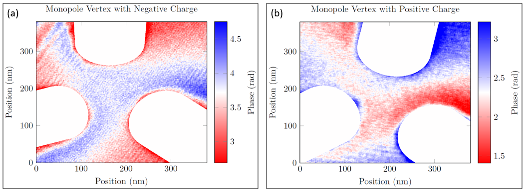
Figure 1. Reconstructed phase maps obtained from vertices in artifical spin ice, with negative (a) and positive (b) charge.
These measurements initially only revealed monopoles with a net charge of Q, but did not reveal any monopoles with a net charge of 3Q. These 3Q monopoles needed to be induced in situ by applying an alternating decaying field in Lorentz mode using the objective lens manually. This allowed individual islands to flip directly along the long axis, creating a small population of 3Q monopoles that could be measured. This ratio of 3Q to Q monopoles was measured to be 3.00 +- 0.2, giving confidence that the sample in question was indeed behaving as an artificial spin ice should.
3.2 Wave Energy Converter Group
3.2.a Full-scale Taper-Ducted OIST-WEC
The first Taper-Ducted OIST- Wave Energy Converter Device is intalled at the Port of Seragaki, home to OIST Marine Science Station, Okinawa. Prior to the installation, the assemby was done on land. The completed structure was then put into the water (along with the floater attached), and towed to the installation location (around 15m off of Seragaki Seawall), using a small boat (Figure 1). A small LED beacon light was also installed on top of the Duct structure to inform passing ship of the location of the structure (Figure 2 (a)). During high tide, especially at night, it is possible for the structure to be completely under water, thus making it difficult to be seen by naked eyes. Furthermore a metal frame was also deployed on the Duct inlet to avoid any large object entering the duct and damaging the turbine. Figure 2 (b) shows the same WEC structure against beraking wave.
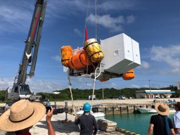
Figure 1. Taper-Ducted OIST - Wave Energy Converter Device surrounded by floaters being lifted into the water using crane to be towed to the installation location using a boat.
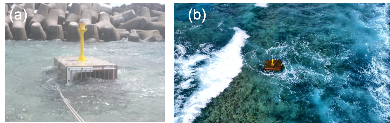
Figure 2. The Taper-Ducted OIST Wave Energy Converter device during the installation (a) and during operation against a breaking wave (b). A yellow LED beacon is installed on top of the structure and metal frame is installed on the inlet of the Duct for safety reasons.
Similar to the monitoring mechanism deployed in Maldives, a power generation measurement system was installed in the pump station facility near the Seragaki seawall (Figure 3). A CCTV camera is installed on the Seragaki's seawall facing the device and the power generation data is uploaded to data storage at OIST via internet connection. The power data then recorded to the cloud storage. During Typhoon Tapah, a peak 6kW of power generation was recorded proving the structure can withstand the extreme weather condition while remains operational.
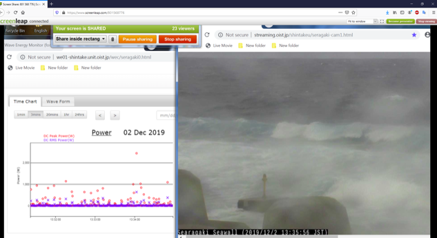
Figure 3. OIST-Wave Energy Converter monitoring screen. A CCTV camera is installed on the Seragaki's seawall facing the device and the power generated data is uploaded to data storage at OIST via cloud storage.
After surviving the Typhoon season aroung the end of 2019, 2 out of 5 turbine blades were found to be failed during a routine expection in January 2020. The exact time of the failure remains unknown at the moment because there was no significant drop in performance found in January. An observation is currently underway to look for the main cause of the failure. It is important to be noted that the same turbine design and material survived over 1 year of operation in the Maldives [1, 2]. With the conclusion of the first complete full-scale Taper-Duct OIST-WEC installation in Okinawa, 4 more devices are currently underway to the Kandooma Beach in Maldives. Figure 4 shows the device being assembled and prepared at Port of Seragaki, before being sent to Maldives by ship. As can be seen from the figure, the event is being televised by local TV station in Okinawa.
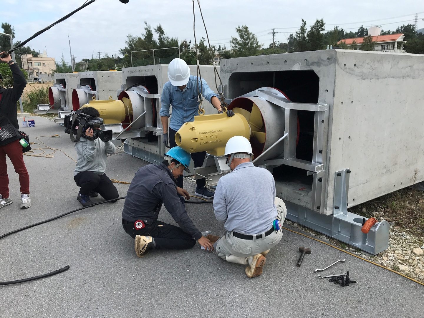
Figure 4. Four (4) Taper-Ducted OIST Wave Energy Converter devices being prepared at the Port of Seragaki before being sent to Kandooma Beach, Maldives, by ship.
[1] Shintake, et al., EWTEC 2019, Italy
[2] Takebe, et al., EWTEC 2019, Italy
3.2.b Large-scale Taper-Duct structure with guide vane study
Due to the explosive nature of breaking wave, a large amount of energy is generated within a fraction of time. Because of this, absorbing the whole energy is challenging given the reaction time of the turbine, especially when the incoming flow is further concentrated by the Taper-Duct structure of the device. To tackle this problem, we try to utilised a guide vane to rotate the incoming flow from the inlet of the Duct to the outlet, before reaching the turbine. Theoretically, by rotating the flow, we will be able to increase the travel time of the water and force the water to hit the turbine blade at the most effective angle [1]. In October 2019, a Half-scale (1:2) physical model testing of this design was tested at Zanpa Beach, Okinawa. A video recording device was utilised to record the water movement inside the Duct, with (Figure 1 (a) and (b)) and without (Figure 1 (c) and (d)) the guide vane. Although an interesting set of data have been produced by the experiment, only a limited observation of flow-structure interaction can be done due to the chaotic nature of breaking wave and insufficient measurement devices. This highlights the needs of more controlled experiments in a lab. The results of the experiment have been presented as posters during the 4th Okinawa Marine Science Workshop in 2019.
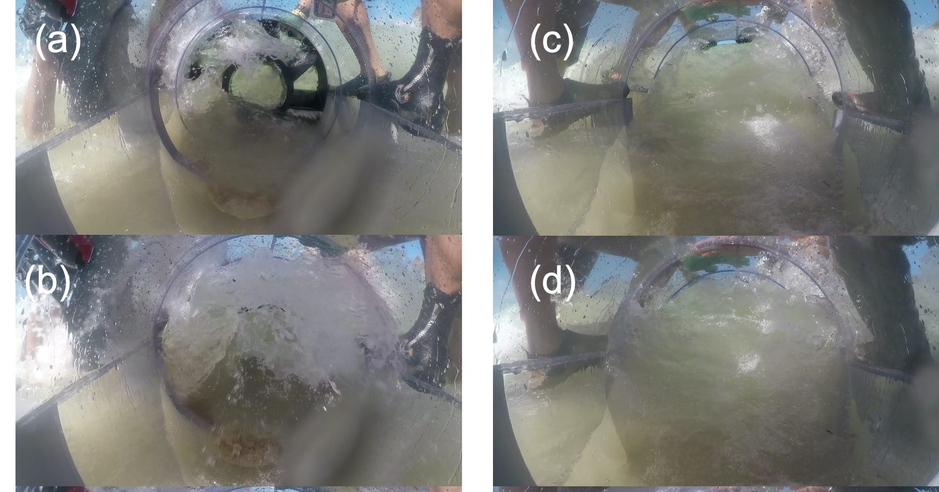
Figure 1. Instantaneous images of Large-scale (1:2) physical model experimental results of the Taper-Duct structure at Zanpa Beach, Okinawa, with the Guide-vane (a) and (b) and without the Guide-Vane (c) and (d). The guide-vane formation is intended to lengthen the travel distance of the water prior to hitting the turbine by rotating the flow. This rotation, furthermore, will force the water to hit the turbine's blade at the most effective angle.
[1] Halder, et al., Energies (2020) 13(4) 996.
3.2.c Small-scale Taper-Duct structure study
Past experiences in conducting real sea experiments highlighted the difficulties related to experiment time planning (weather window) and how to get the measurements. At one instance, we were forced to called-off an experiment on-site because the sea condition was deemed too dangerous by the team leader. This came after the same experiment was delayed for about a week due to the bad weather. Because of this, we find the need to have a small-scale (about 1:20) experimental flume inside OIST. This is intially an intern project but later continued to be part of a continuous project. The project is to build a small wave flume which can accommodate a small-scale physical model of the Taper-Duct testing against a breaking wave. The initial design consist of a 1.0m x 0.5m x 0.2m water tank, a wave paddle at one end, wave absorption foam at the other end, and a beach model loosely based on Port of Seragaki's bathymetry. The wave paddle later upgraded to be motorised, so stable breaking wave can be generated and controlled. Furthermore, a clear small-scale physical model (1:20) of the duct was made using acrylic material to ensure a clear observation from all angle. Figure 1 shows an example of the small-scale model experiment being done. In order to improve the measurement quality, a couple fo pressure sensors have been purchased and are currently being installed in the flume.
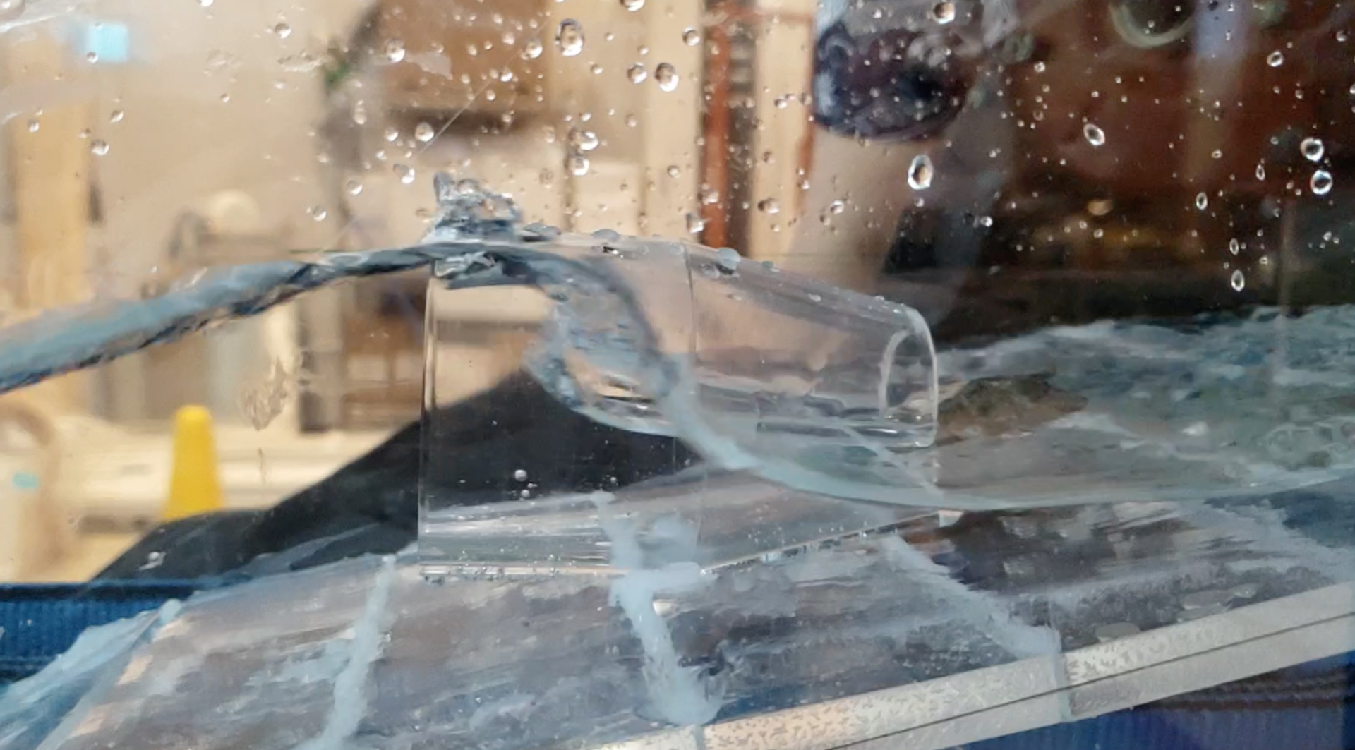
Figure 1. Small scale (1:20) physical model of the Taper-Duct experiments using the small wave flume at OIST against regular breaking wave. A motorised wave paddle is utilised to generate the breaking wave.
4. Publications
4.1 Journals
"Proximity proteomics identifies cancer cell membrane cis‐molecular complex as a potential cancer target."
Norihiro Kotani, Arisa Yamaguchi, Tomoko Ohnishi, Ryusuke Kuwahara, Takanari Nakano, Yuka Nakano, Yui Ida, Takayuki Murakoshi, Koichi Honke
Cancer Science (2019) 110 (8): 2607-2619. doi: doi.org/10.1111/cas.14108
"Low-energy in-line electron holographic imaging of vitreous ice-embedded small biomolecules using a modified scanning electron microscope."
Martin Cheung, Hidehito Adaniya, Cathal Cassidy, Masao Yamashita, Tsumoru Shintake
Ultramicroscopy (2020) 209 (2): 112883. doi: 10.1016/j.ultramic.2019.112883
"Turbine Characteristics of Wave Energy Conversion Device for Extraction Power Using Breaking Waves"
Paresh Halder, Hideki Takebe, Krisna Pawitan, Jun Fujita, Shuji Misumi, Tsumoru Shintake
Energies (2020) 13(4) 996 doi: 10.3390/en13040966
4.2 Books and other one-time publications
Nothing to report
4.3 Oral and Poster Presentations
- "Electron holography studies of CdTe devices"
Cathal Cassidy, Hidehito Adaniya, Shinichiro Takeda, Tadayuki Takahashi, Tsumoru Shintake
Canadian Summer School in Electron Microscopy, June 5, 2019, Hamilton, Ontario, Canada - "Preliminary Study on in vacuo Preparation of TEM Specimens by Electrospray Molecular Deposition System"
Masao Yamashita, Jun Fujita, Kunihiro Aoshima, Seita Taba and Tsumoru Shintake
The 75th Annual Meeting of the Japanese Society of Microscopy, June 17-19, 2019, Nagoya, Japan - "Structural analysis of alpha-mannosidase"
Ryusuke Kuwahara, Ryo Misaki, Kazuhito Fujiyama, Tsumoru Shintake
The 75th Annual Meeting of the Japanese Society of Microscopy, June 18, 2019, Nagoya, Japan - "Imaging Monopoles in Spin Ice via Electron Holography"
Ankur Dhar
SLAC National Accelerator Laboratory, August 15, 2019, USA - "Exploration of Bragg inline holography as a potential tool for crystal structure determination"
Cathal Cassidy, Tatiana Latychevskaia, Tsumoru Shintake
ECM32 (European Crystallography Meeting), August 22, 2019, Vienna, Austria - "Results of Wave Energy Experiments in the Maldives"
Tsumoru Shintake, Katsutoshi Shirasawa, Jun Fujita, Shuji Misumi, Paresh Halder,Tamotsu Nagahama, Toshio Shindou, Hamish Taggart, Hikaru Kamimura and Hideki Takebe,
EWTEC2019, The 13th European Wave and Tidal Energy Conference, September 1-6, 2019, Napoli, Italy - "Wave Power Measurement at Breaking Wave Zone in Maldives using Horizontal-Axis Turbine WEC”
Hideki Takebe, Katsutoshi Shirasawa, Jun Fujita, Shuji Misumi, Paresh Halder and Tsumoru Shintake
EWTEC2019, The 13th European Wave and Tidal Energy Conference, September 1-6, 2019, Napoli, Italy. - "Electron holography studies of CdTe & devices”
Cathal Cassidy, Tsumoru Shintake
Hitachi Centre for Exploratory Research (Hatoyama, "Tonomura microscope"), Oct 18, 2019. - "Electron holography studies of next-generation medical imaging sensor materials”
Cathal Cassidy, Hidehito Adaniya, Tsumoru Shintake (OIST), S. Takeda, T. Takahashi (U Tokyo), M. Ageishi, D. Morikawa, K. Tsuda (Tohoku University), T. Akashi, H. Kasai, H. Shinada (Center for Exploratory Research, Hitachi).
OIST-Ryudai Symposium: Medical Sciences: basic medical science to clinical medecine), Dec 16, 2019 (OIST). - "Computational study of Wave breaking Turbine for wave energy conversion"
Paresh Halder, Tsumoru Shintake at 4th Okinawa Marine Science Workshop, December 2019 (OIST). - "Empowering the world through the ocean: Surf-zone WEC, from paper to reality"
Krisna Pawitan, Hanley Andrean, Paresh Halder, Hideki Takebe, Jun Fujita, Shuji Misumi, Tsumoru Shintake at 4th Okinawa Marine Science Workshop, December 2019 (OIST). - "Redistributing power spike on OIST WEC with a guide vane: preliminary experiment"
Hanley Andrean, Krisna Pawitan, Paresh Halder, Hideki Takebe, Jun Fujita, Shuji Misumi, Tsumoru Shintake at 4th Okinawa Marine Science Workshop, December 2019 (OIST). - "Numerical Study of OIST Wave Energy Generation"
Fuad Assidiq, Krisna Pawitan, Paresh Halder, Hideki Takebe, Jun Fujita, Shuji Misumi, Tsumoru Shintake at 4th Okinawa Marine Science Workshop, December 2019 (OIST). - "Electron microscopy research @ Shintake unit (OIST)”
Cathal Cassidy, Hidehito Adaniya, Martin Cheung, Masao Yamashita, Tsumoru Shintake
OIST-Hitachi Joint Symposium 2020, Feb 17th 2020 (Hitachi Central Research laboratory "Kyousou no Mori", Tokyo).
5. Intellectual Property Rights and Other Specific Achievements
Nothing to report
6. Meetings and Events
6.1 Physical principles underlying operation of phase plates in a TEM
- Date: November 18, 2019
- Venue: OIST Campus Lab1
- Speaker: Dr. Marek Malac (National Research Council Canada | NRC · National Institute for Nanotechnology| NINT)
6.2 Sustainability of wave energy resources in Northeast Asia
- Date: December 5, 2019
- Venue: OIST Campus Lab1
- Speaker: Dr. Bahareh Kamranzad (The Hakubi Center for Advanced Research, Kyoto University)
7. Other
7.1 Outreach
- High school talk (18th Feb 2020)
- Audience: Itoman Junior High School (~90 students, OIST B250)
- Title: "My life as a Scientist"
- Speaker: Dr. Martin Cheung.
- Middle school talk (26th Feb 2020)
- Venue: Hope International Academy Okinawa (Chatan)
- "Careers in Science & Technology" (2 hour seminar for middle school students discussing career options and higher education choices)
- Speaker: Dr. Cathal Cassidy
7.2 Media
- The installation of Taper-Ducted OIST Wave Energy Converter device at the Port of Seragaki was featured on Okinawa TV (OTV) on Thursday, July 12th 2019. (20190711-OTV-河川・環境シリーズ-沖縄発の波力発電実用化へ)
7.3 Covid19 activities
- arXiv preprint
- Title: "Possibility of Disinfection of SARS CoC-2 (COVID-19) in Human respiratory Tract by Controlled Ethanol Vapor Inhalation".
- Prof. T. Shinake.
- Link: https://arxiv.org/abs/2003.12444