

Technician - Device Fabrication and Characterization
Postion Description: The Femtosecond Spectroscopy (Dani) Unit at OIST is recruiting researchers or technicians in the broad area of ‘fabrication and characterization of opto-electronic devices and van der Waals heterostructures’. Over the past seven years, the unit has developed pioneering capabilities in studying materials via time-resolved photoemission microscopy [1,2] and various ultrafast spectroscopy techniques [3, 4]. The successful candidates will support efforts in the fabrication and characterization of opto-electronic devices and van der Waals heterostructures. Opportunities to contribute to the ongoing science will be significant, including the possibility to lead projects.
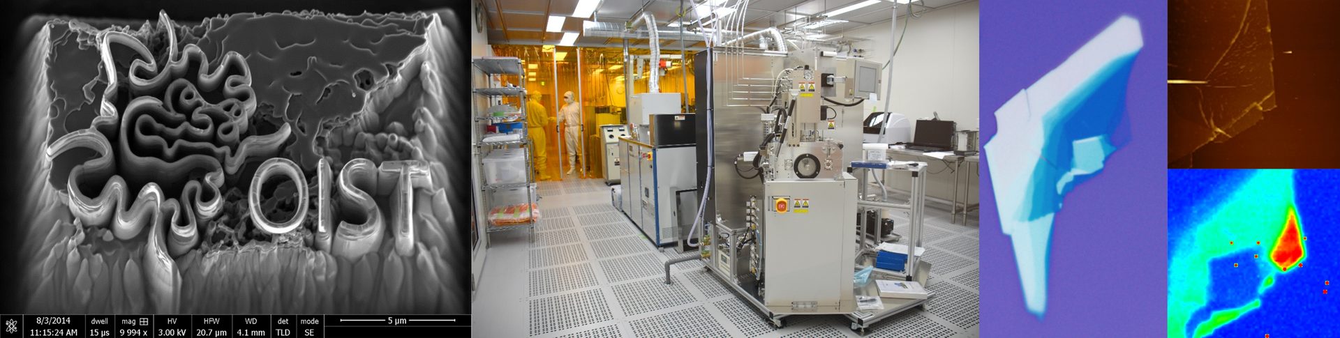
The successful candidates will leverage and work with the unit’s state-of-the-art experimental laboratories including multiple kHz, 100-kHz and MHz class amplified, ultrafast lasers, multiple ultrafast oscillator systems, a low-energy electron microscope and photoemission electron microscope (LEEM/PEEM), time-of-flight based Momentum Microscope (METIS-TOF) and a 17 T cryo-free superconducting magnet for nonlinear optical & THz measurements. First-rate shared institute facilities for material characterization (including Raman, Photoluminescence, FTIR, XRD, XPS, SEM, high res. TEM) and nanofabrication (including state-of-the-art clean rooms, e-beam and photo-lithography, FIB-SEM, ALD, deposition systems) are also available.
Interaction opportunities exist with various international institutes, including Stanford Univ. (California, USA), Rice Univ. (Houston, Texas, USA), École Normale Supérieure (Paris, France), TIFR (Mumbai, India) and Univ. of Cambridge (UK).
Qualifications: Candidates will be considered at all levels, including bachelors, masters and PhD, with compensation and responsibilities commensurate with experience. Previous experience in device or materials fabrication and characterization, particularly van der Waals materials, is important, particularly for the more senior candidates.
Compensation and Benefits: In line with the values at OIST we are committed to attracting top-class researchers from across the world, and to ensuring a supportive, creative and productive atmosphere for them and their families. The final compensation package will take into consideration the candidates’ experience and background and will be competitive with international standards. Conversion to a long term position is also a possibility.
Application Instructions: Please submit (i) a brief cover letter, stating your motivation to apply, (ii) your CV, including publication list, and (iii) contact information of upto two references to recruiting-FSU@oist.jp. Short listed candidates may be invited for an interview to OIST. Applications will be reviewed as received.
References:
[1] Imaging the motion of electrons across semiconductor heterojunctions, Nat. Nanotechnol. 12, 36 (2017). Cover Jan 2017 Edition.
[2] Pulling apart photoexcited electrons by photoinducing an in-plane surface electric field, Science Advances 4, eaat9722 (2018).
[3] High-temperature terahertz optical diode effect without magnetic order in polar FeZnMo3O8, Phys. Rev. Lett. 120, 037601 (2018).
[4] Ultrafast charge transfer and enhanced absorption in MoS2 - organic van der Waals heterojunctions using plasmonic metasurfaces, ACS Nano 10, 9899 (2016).