

FY2015 Annual Report
Femtosecond Spectroscopy Unit
Assistant Professor Keshav Dani
Abstract
In recent years, the ability to synthesize, engineer & observe materials on the nanometer length scale has led to novel phenomena and applications. On the other hand, modern lasers deliver powerful, ultrashort pulses of light allowing us to observe the interaction of electrons and atoms on the femtosecond timescale. Together, these technologies allow us to study new paradigms in light-matter interaction – with femtosecond temporal resolution and nanometer spatial resolution. In FY2015, Femtosecond Spectroscopy Unit has directed these abilities and made progress towards two different areas of study:
(a) Novel two-dimensional materials and their heterostructures, where we search for new functionality in materials with applications in optics, electronics and energy;
(b) Terahertz devices & applications, where we investigate the generation of broadband THz radiation and applying this to a variety of materials and devices.
1. Staff
- Dr. Keshav M. Dani, Professor
- Dr. Michael K. L. Man, Researcher
- Dr. Bala Murali Krishna, Researcher
- Dr. Takaaki Harada, Researcher
- Dr. Eleftheria Kavousanaki, Researcher
- Dr. Julien Madéo, Researcher
- E Laine Wong, Graduate Student
- Viktoras Lisicovas, Graduate Student
- Andrew Winchester, Graduate Student
- Athanasios Margiolakis, Special Research Student
- Shiho Saito, Administrative Assistant
- Yumi Ito, Administrative Assistant
2. Collaborations
Theme: Novel two-dimensional materials and their heterostructures
- Type of collaboration: Joint research
- Researchers:
- Professor S. Talapatra, Southern Illinois Univ., Carbondale, IL, USA
- Professor S. Kar, Northeastern University, Boston, MA, USA
- Professor P.M. Ajayan, Rice University, Houston, TX, USA
- Dr. Robert Vajtai, Ricer University, Houston, TX, USA
- Professor D. Talbayev, Tulane University, New Orleans, LA, USA
- Prof. Angel Rubio, Universidad del Pais Vasco, San Sebastian, Spain
- Professor E. Kioupakis, University of Michigan, MI, USA
- Professor M. Terrones, Pennsylvania State University, PA, USA
- Dr. A.D. Mohite, Los Alamos National Lab, Los Alamos, NM, USA
- Dr. G. Gupta, Los Alamos National Lab, Los Alamos, NM, USA
Theme: Terahertz Devices and Applications
- Type of collaboration: Joint research
- Researchers:
- Professor Z.-Y. Zhao, Shanghai Normal University, Shanghai, China
- Professor Q.-Z. Zhao, Shanghai Normal University, Shanghai, China
- Professor W. Peng, Shanghai Normal University, Shanghai, China
- Professor W.-Z. Shi, Shanghai Normal University, Shanghai, China
3. Activities and Findings
3.1 Novel Two-Dimensional Materials and Their Heterostructures
Since the discovery of Graphene in 2004, the study of two-dimensional (2D) materials and their heterostructures has spawned a new field of condensed matter physics. Understanding the optical properties of these new materials, their nonlinear interaction with light, and the light-induced ultrafast dynamics of electrons in these materials has been one of the main research thrusts of the unit. In continuation of the work from previous years, the unit has made progress in the following areas in FY2015:
A. Observing the interplay between surface and bulk nonlinearities in thin van der Waals crystals
Over the past decade, van der Waals (vdW) crystals have provided a rich playground in the exploration of physical phenomena through the transition from 3D bulk crystals to 2D atomically thin layers. For example, graphene – monolayers of graphite – exhibit charges with a relativistic dispersion [1] and transition metal dichalcogenides, such as MoS2, exhibit a strong photoluminescence owing to the emergence of a direct bandgap at the monolayer limit [2]. Beyond those considerations, exploring the optical nonlinearities of vdW materials and how the reduced dimensionality impacts the nonlinear optical properties is important both from a fundamental aspect as well as for their integration in optoelectronic devices. In FY2015, the unit has investigated nonlinear wavelength conversion in thin van der Waals crystals in order to understand the impact of the 3D to 2D transition on optical nonlinearities, namely the interplay between surface and bulk nonlinearities (Fig.1) [3].
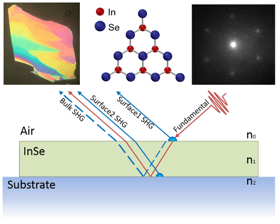
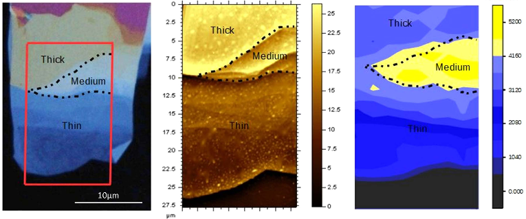
We have studied exfoliated InSe [4], a III-VI van der Waals crystal and close cousin of GaSe for which the highest second order nonlinearities have been reported [5]. We have investigated the evolution of second harmonic generation (SHG) by pumping the material below the bandgap using 150 fs excitation through a microscope. This allowed us to map the SHG intensity across the sample composed of thicknesses ranging from 9 to 25 nm (Fig.2). Instead of the expected quadratic dependence on the SHG with propagation length, we observed a periodic modulation of the SHG intensity versus thickness. We have attributed this phenomenon to an interference effect between surface and bulk nonlinearities in good agreement with our theoretical model. Our results show that thin vdW crystals allow for the interplay between comparable surface and bulk nonlinear contributions. It demonstrates the ability to engineer the nonlinearities by manipulating the relative phase of the two contributions by tuning the bulk thickness or selecting substrates and capping layers with different dielectric properties. This has direct implications in the integration of vdW crystals in nano-scale optoelectronic devices.
References Section 3.1 A:
[1] A. K. Geim, and K. S. Novoselov, The rise of graphene, Nat. Mater. 6, 183-191 (2007).
[2] K. F. Mak, et al. Atomically thin MoS2: a new direct-gap semiconductor, Phys. Rev. Lett. 105, 136805 (2010).
[3] S. Deckoff-Jones, et al. Observing the interplay between surface and bulk optical nonlinearities in thin van der Waals crystals, Sci. Rep. 6, 22620 (2016).
[4] S. Lei, et al. Evolution of the electronic band structure and efficient photodetection in atomic layers of InSe, ACS Nano 8, 1263-1272 (2014).
[5] X. Zhou, et al. Strong second harmonic generation in atomic layered GaSe, J. Am. Chem. Soc. 137, 7994-7997 (2015).
B. Chemical vapor deposition synthesized atomically-thin Molybdenum Disulfide with optoelectronic-graded crystalline quality
Monolayer molybdenum disulfide (MoS2) is an emerging novel material with interesting optical and transport properties, with potential future applications. There is a large push to adapt methods such as chemical vapor deposition (CVD) to produce samples on large scales, which will enable mass production of optoelectronic devices. In order to evaluate the quality of samples grown by CVD, complimentary methods which together cover transport, optical and crystal structure properties are needed. The work done by FSU towards this research [1] consisted of Raman and photoluminescence (PL) characterization of MoS2 crystals grown by CVD. These optical methods give complimentary information about crystal quality and optical properties. FSU performed spatially resolved Raman and PL maps of crystals in order to show the homogeneity of the vibrational properties and photoluminescence emission of individual single crystals. The uniform intensity of the E12g and A1g Raman modes as well as the PL emission showed that the crystal maintains its quality over the entire sample. Further, the constant difference in frequency between the E12g and A1g Raman modes of ~17 cm-1 over the sample showed that the flake was of uniform monolayer thickness, which is also supported by the strong photoluminescence emission characteristic of monolayer samples. Together, this proved that the CVD process used was able to produce crystals of high quality over sizes of tens of micrometers.
References Section 3.1 B:
[1] I. Bilgin, et al. Chemical vapor deposition synthesized atomically-thin Molybdenum Disulfide with optoelectronic-graded crystalline quality, ACS Nano 9, 8822 (2015).
C. Ultrafast intrinsic photoresponse and direct evidence of sub-gap states in liquid phase exfoliated MoS2 thin films
Two-Dimensional structures with swift optical response have several technological advantages, for example they could be used as components of ultrafast light modulators, photo-detectors, and optical switches. Among the existing sample fabrication techniques, liquid phase exfoliation is considered to be the most suitable method for achieving large scale and low cost synthesis of 2D materials. We report on the fast photo switching behavior of thin films of liquid phase exfoliated MoS2, when excited with a continuous laser of λ= 658 nm, over a broad range of laser power. Transient Terahertz (THz) photo-conductivity measurements, using an optical pump and THz probe (OPTP), reveal that photo carrier decay follows a bi-exponential time dependence, with decay times of the order of picoseconds, indicating that the photo carrier recombination occurs via trap states. The nature of variation of photocurrent with temperature confirms that the trap states are continuously distributed within the mobility gap in these thin films of MoS2, and play a vital role in influencing the overall photo response. Our findings provide a fundamental understanding of the photo-physics associated with optically active 2D materials and are crucial for developing advanced optoelectronic devices.
References Section 3.1 C:
[1] S. Ghosh, et al. Ultrafast intrinsic photoresponse and direct evidence of sub-gap states in liquid phase exfoliated MoS2 thin films, Sci. Rep. 5, 11272 (2015).
D. Engineering photophenomena in large, three dimensional structures composed of self-assembled van der Waals heterostructure flakes
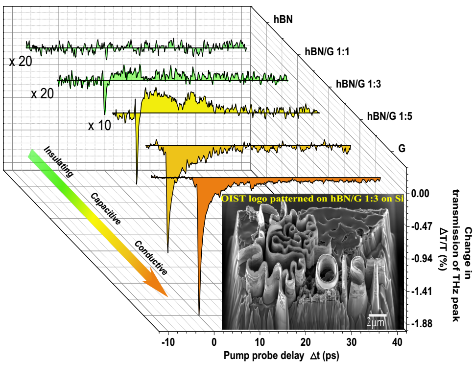
Van der Waals heterostructures, made of few-layer assemblies of two-dimensional materials have shown promise for nanoscale opto-electronic devices, but remain limited in size, dimensionality and scalability. Newly emerging ideas suggest the assembly of different 2D materials into heterostructures via van der Waals bonding to obtain a near limitless combination of materials capabilities and unexplored functionalities. We demonstrate for the first time scalable, micron-sized, robust 3D van der Waals heterostructures – three orders of magnitude larger than previous reports, made by self-assembling atomically-thin flakes of hexagonal Boron Nitride (hBN) and Graphene (G) in varying ratios. Driven by hBN/G interface interactions, we see the emergence of a dissipationless, purely capacitive photoresponse in the terahertz (THz), distinct from that of the parent materials. We engineer this photoresponse over an unprecedented range – insulating to capacitive to conductive, simply by varying the heterostructure composition shown in the figure 3, an unfeasible possibility in few-layer devices. Such heterostructures have broad implications for tunable opto-electronic materials, enhancement of interface properties for solar cell and photodetector applications, and in the fabrication of other 3D van der Waals solids exhibiting new physical phenomena.
References Section 3.1 D:
[1] B. M. K. Mariserla, et al. Engineering photophenomena in large, three dimensional structures composed of self-assembled van der Waals heterostructure flakes, Adv. Opt. Mater. 3, 1551 (2015).
E. Protecting the properties of monolayer MoS2 with an atomically thin buffer
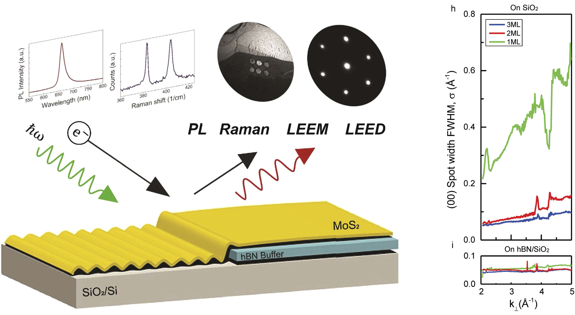
Graphene-like 2D materials, such as transition metal dichalcogenides (TMDs), have gained much attention due to their potential in opto-electronic device applications. However, like graphene and other atomically thin materials, TMDs lose their key properties when they are being placed on a supporting substrate. For example, we observed quenching of photoluminescence intensity, distortion of crystalline structure, and roughening of surface morphology in molybdenum disulfide (MoS2), when we place MoS2 onto Si-based substrates. The ability to protect these properties in TMDs on standard Si-based substrates, will enable their use in opto-electronic devices and scientific investigations. In our study, we show that an atomically-thin buffer of hBN is enough to protect the structural, morphological and opto-electronic properties of MoS2 (Fig. 4). Compared to bare Si, the hBN buffer improves by over an order of magnitude the surface roughness, the lattice structure, and the photoluminescence. This scheme provides a way to integrate monolayer MoS2 onto other substrates without compromising their unique properties, as well as allow the integration of other 2D materials into the technologically viable Si-substrates.
References Section 3.1 E:
[1] M. K. L. Man, et al. Protecting the properties of monolayer MoS2 on silicon based substrates with an atomically thin buffer, Sci. Rep. 6, 20890 (2016).
3.2 Terahertz Devices and Applications
A. Ultrafast properties of femtosecond-laser-ablated GaAs and its application to terahertz optoelectronics
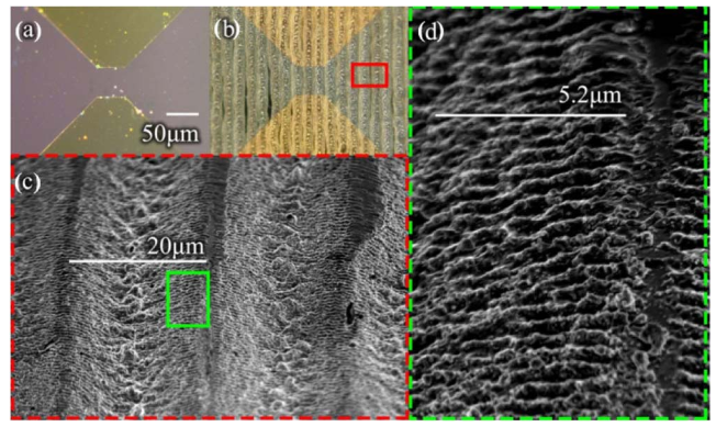
The terahertz (THz) region of the electromagnetic spectrum covers an important frequency range at the interface between electronics and photonics [1]. Over the past decade, many significant scientific and technological applications have emerged for this range such as investigation of low energy interactions in materials [2], imaging techniques [3] and security applications [4]. Despite wide ranging applications, the THz range suffers from a lack of efficient and compact sources and detectors. In previous years, the unit has demonstrated novel THz sources [5] based on semiconductor materials. In FY2015, the unit has developed a method based on a controlled femtosecond-laser-ablation of a surface to enhance the optoelectronic properties of a semiconductor material (e.g. absorption) allowing to achieve THz sources with improved emission [6].
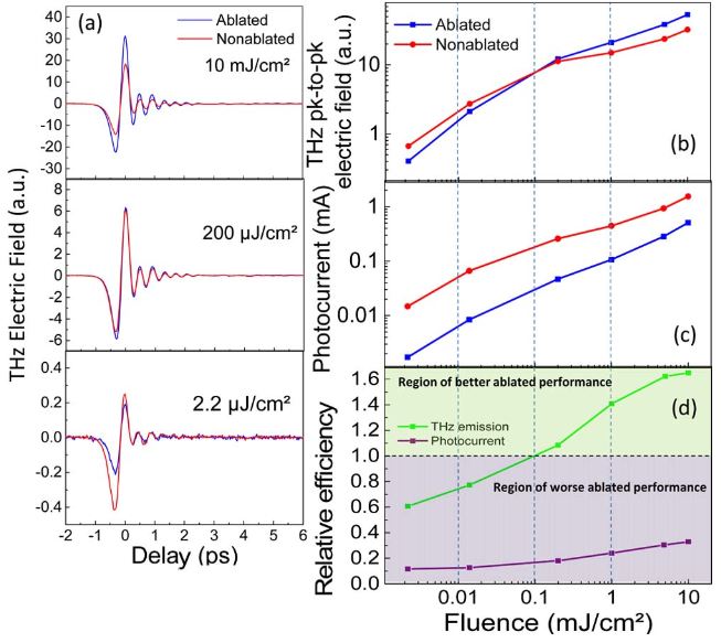
In recent years, irradiation by intense ultrashort laser pulses has led to the demonstration of enhancement of material optical and electronic properties [7]. This technique allows the realization of new electronic surface states as well as a broad variety of micro- and nano-structured texturization. This method has been used on silicon to achieve hyperdoping allowing for close 100% absorption of light over a wider spectral range than the intrinsic material [8]. We have applied femtosecond-laser-ablation on GaAs in order create a periodic subwavelength pattern (Fig.5) which results in a dramatic change of the optoelectronic response and characteristics of the material. In particular, it shows close to 100% absorption, n-doping and picosecond carrier lifetime. We have used the ablated GaAs to fabricate photoconductive antennas - a coherent THz source converting NIR ultrashort pulses into THz pulses - and have compared its emission with a photoconductive antenna made of the bare material with THz Time-Domain Spectroscopy. Our results show a more than 60% enhancement of the emission (Fig.6) from the femtosecond-laser-ablated device attributed to the high absorption. Our work demonstrates that this laser based process is a powerful tool to engineer material properties such as doping, photoabsorption and carrier lifetime opening a new route toward cost-effective and efficient THz devices.
References Section 3.2 A:
[1] M. Tonouchi, Cutting-edge terahertz technology, Nat. Photonics 1, 97-105 (2007).
[2] P. U. Jepsen, et al. Terahertz spectrocoscopy and imaging, Laser & Photonics Reviews 5, 124-166 (2011).
[3] D. A. Usanov, et al. Terahertz waves and perspectives of terahertz biomedical technologies development, MIKON 2008 - 17th International Conference on Microwaves, Radar & Wireless Communications, Wroclaw, 1-10 (2008).
[4] J. F. Federici, et al. THz imaging and sensing for security applications -explosives, weapons and drugs, Semicond. Sci. Technol. 20, 50-58 (2012).
[5] P. J. Hale, et al. 20 THz broadband generation using semi-insulating GaAs interdigitated photoconductive antennas, Optics Express 22, 26358 (2014).
[6] J. Madéo, et al. Ultrafast properties of femtosecond-laser-ablated GaAs and its application to terahertz optoelectronics, Optics Lett. 40, 3388-3391 (2015).
[7] C. R. Phipps, Laser ablation and its applications, Optical Sciences (Springer, 2007).
[8] M.-J. Sher, et al. Pulsed-laser hyperdoping and surface texturing for photovoltaics, MRS Bulletin 36, (2011).
4. Publications
4.1 Journals
- S. Deckoff-Jones, J. Zhang, C. E. Petoukhoff, M. K. L. Man, S. Lei, R. Vajtai, P. M. Ajayan, D. Talbayev, J. Madéo and K. M. Dani, Observing the interplay between surface and bulk optical nonlinearities in thin van der Waals crystals, Sci. Rep. 6, 22620 (2016).
- M. K. L. Man, S. Deckoff-Jones, A. Winchester, G. Shi, G. Gupta, A. D. Mohite, S. Kar, E. Kioupakis, S. Talapatra and K. M. Dani, Protecting the properties of monolayer MoS2 on silicon based substrates with an atomically thin buffer, Sci. Rep. 6, 20890 (2016).
- C. E. Petoukhoff, C. Antonick, B. M. K. Mariserla, K. M. Dani and D. M. O'Carroll, Oxidation of planar and plasmonic Ag surfaces by exposure to O2/Ar plasma for organic optoelectronic applications, MRS Advances 1, 943 (2016).
- I. Bilgin, F. Kiu, A. Vargas. A. Winchester, M. K. L. Man, M. Upmanyu, K. M. Dani, G. Gupta, S. Talapatra, A. D. Mohite, S. Kar, Chemical vapor deposition synthesized atomically-thin Molybdenum Disulfide with optoelectronic-graded crystalline quality, ACS Nano 9, 8822 (2015).
- B. M. K. Mariserla, M. K. L. Man, S. Vinod, C. Chin, T. Harada, J. Taha-Tijerina, C. S. Tiwary, P. Nguyen, P. Chang, T. N. Narayanan, A. Rubio, P. M Ajayan, S. Talapatra and K. M. Dani, Engineering photophenomena in large, three dimensional structures composed of self-assembled van der Waals heterostructure flakes, Adv. Opt. Materials 3, 1551 (2015).
- S. Ghosh, A. Winchester, B. Muchhaarla, M. Wasala, S. Feng, A. L. Elias, B. M. K. Mariserla, T. Harada, C. Chin, K. M. Dani, S. Kar, M. Terrones, and S. Talapatra, Ultrafast intrinsic photoresponse and direct evidence of sub-gap states in liquid phase exfoliated MoS2 thin films, Sci. Rep 5, 11272 (2015).
- J. Madeo, A. Margiolakis, Z.-Y. Zhao, P. J. Hale, M. K. L. Man, Q.-Z. Zhao, W. Peng, W.-Z. Shi and K. M. Dani, Ultrafast properties of femtosecond-laser-ablated GaAs and its application to terahertz optoelectronics, Opt. Lett 40 (14), 3388-3391 (2015).
- D. Palaferri, Y. Todorov, Y. N. Chen, J. Madéo, A. Vasanelli, L. H. Li, A. G. Davies, E. H. Linfield, and C. Sirtori, Patch antenna terahertz photodetectors, Appl. Phys. Lett 106, 161102 (2015).
4.2 Books and Other One-Time Publications
Nothing to report.
4.3 Oral and Poster Presentations
- Mariserla, B. M. K., Man, M. K. L., Vinod, S., Chin C., Harada T., Taha-Tijerina, J., Tiwary C. S., Nguyen, P., Chang, P., Narayanan, T. N., Pubio, A., Ajayan, P. M., Talapatra, S., Dani, K. M. Emergent photophenomena in three dimensional van der Waals heterostructures, Oral Presentation, CLEO 2015 Jan Jose, CA, USA, May 10-15 (2015).
- Petoukhoff, C. E., Voiry, D., Mariserla, B. M. K., Bozkurt, I., Chhowalla, M., O’Carroll, D., Dani, K. M. Investigating the Ultrafast Charge Dynamics in Polymer Solar Cells Incorporating Passivated Metasurfaces, Poster Presentation, Japanese Society for the Promotion of Science Summer Fellowship Meeting, Soken University, Japan, Jun 12 (2015).
- Mariserla, B. M. K., Man, M. K. L., Vinod, S., Chin, C., Harada, T., Taha-Tijerina, J., Tiwary, C. S., Nguyen, P., Chang, P., Narayanan, T., Rubio, A., Ajayan, P., Talapatra, S., Dani, K. M. Engineering photophenomena in self-assembled 3D van der Waals heterostructures, Oral Presentation, ICMAT 2015, Sunte, Singapore, Jun 28–Jul 03 (2015).
- Dani, K. M. Terahertz opto-electronic properties of femtosecond-laser-ablated GaAs, Invited Talk, MTSA 2015 and TraNano-6, Okinawa Institute of Science and Technology Graduate University Okinawa, Japan, Jun 30-Jul 04 (2015).
- Gilman, A., Dani, K. M. Quantum Cascade Lasers and Terahertz Technology, Oral Presentation, MTSA Student Workshop, Okinawa Institute of Science and Technology Graduate University Okinawa, Japan, Jun 30 – Jul 04 (2015).
- Renaud, D. Dani, K. M. Protecting the Optical Properties of Atomically Thin Black Phosphorous, Oral Presentation, MTSA Student Workshop, Okinawa Institute of Science and Technology Graduate University Okinawa, Japan, Jun 30-Jul 04 (2015).
- Renaud, D., Deckoff-Jones, S., Zhang, J., Man, M. K. L., Dani, K. M. Protection of the Optical Properties of Few Layer 2D Phosphane, Poster Presentation, MTSA Student Workshop, Okinawa Institute of Science and Technology Graduate University Okinawa, Japan, Jun 30- Jul 04 (2015).
- Dani, K. M. Emergent photophenomena in 3D structures composed of van der Waals heterostructure flakes, Invited Talk, Physical Science Symposium on: Quantum Science & Crystal/Graphene Science, Cambridge, MA, USA, Sep 21-22 (2015).
- Renaud, D., Dani, K. M. Protection of the Optical Properties of Few Layer 2D Phosphane, Poster Presentation, SHPE Conference 2015, Baltimore, USA, Nov 11-15 (2015).
- Mariserla, B. M. K., Dani, K. M. Emergent photophenomena in three dimensional van der Waals heterostructures, Oral Presentation, EMN meeting on Ultrafast Research 2015, Las Vegas, USA Nov 16-19 (2015).
- Man, M. K. L., Deckoff-Jones, S., Harada, T., Wong, E., Margiolakis, A., Krishna, M. B. K., Madeo, J., Winchester, A., Lei, S., Vajtai, R., Ajayan, P. M., Dani, K. M. Visualization of photo-excited electrons in 2D Indium Selenide nanoflakes, Poster Presentation, FOCUS PEEM Workshop 2015 Hunstetten, Germany, Nov 18-20 (2015).
- Dani, K. M., Mariserla, B. M. K., Chin, C., Harada, T., Vinod, S., Taha-Tijerina, J., Nguyen, P., Narayanan, T. N., Ajayan, P. M., Man, M. K. L, Madeo, J. Opto-electronic phenomena in large, 3D structures composed of few-layer van der Waals heterostructures, Invited Talk, International Symposium on Functional Materials (ISFM2016), Okinawa Institute of Science and Technology Graduate University Okinawa, Japan, Jan 25-29 (2016).
- Petoukhoff, C. E., Mariserla, B. M. K., Voiry, D., Bozkurt, I., Deckoff-Jones, S., Chhowalla, M., O’Carroll, D. M., Dani, K. M. Enhanced Absorption and Charge Photogeneration in Polymer:Fullerene Thin-Films with MoS2-Metasurface Heterostructures, Oral Presentation, 2016 MR, Phoenix, AZ, USA., Mar 28– Apr 01(2016).
5. Intellectual Property Rights and Other Specific Achievements
Nothing to report.
6. Meetings and Events
6.1 Seminar
- Date: June 15th 2015
- Venue: OIST Campus Center
- Speaker: Dr. Matteo Rini
- Date: July 22nd 2015
- Venue: OIST Campus Lab3
- Speaker: Prof. Kenneth Burch
- Date: October 30th 2015
- Venue: OIST Campus Lab1
- Speaker: Prof. Stephane Tombet
6.2 Workshop
Joint Symposium of 3rd International Symposium on Microwave/THz Science and Applications (MTSA 2015) and 6th International Symposium on Terahertz Nanoscience (TeraNano-6)
- Date: June 30- July 4 (2015)
- Venue: OIST Campus, Auditorium, R&D Cluster Hall, and C210 (Center Buld)
- Organizers: Masayoshi Tonouchi(RIKEN, Japan), Chiko Otani (Osaka Univ., Japan), Keshav Dani (OIST, Japan)
- Plenary Speakers:
- Dr. Martin Koch (Philipps Univ. Germany)
- Dr. Xi-Cheng Zhang (Rochester Univ. USA)
- Invited Speakers
- Dr. Masahiro Asada (Tokyo Inst. Tech., Japan)
- Dr. Masaaki Ashida (Osaka Univ., Japan)
- Dr. Takashi Arikawa (Kyoto Univ., Japan)
- Dr. Rene Beigang (Fraunhofer IPM, Germany)
- Dr. Jian Chen (Nanjing Univ., China)
- Dr. Hyunyoung Choi (Yonsei Univ., S. Korea)
- Dr. Sukhdeep S. Dhillon (CNRS/Ecole Normale Superieure, France)
- Dr. Sebastian Diebold (Osaka Univ., Japan)
- Dr. Cathy Forey (CSIRO, Austraria)
- Dr. Jinguang Han (Tianjin Univ., China)
- Dr. Frank Hegmann (Univ. Alberta, Canada)
- Dr. Kenji Ikushima (Tokyo Univ. Agri. Tech., Japan)
- Dr. Young Uk Jeong (KAERI, South Korea)
- Dr. Peter Uhd Jepsen (Technical Univ. Denmark, Denmark)
- Dr. Michael Johnston (Univ. Oxford, UK)
- Dr. Hiromichi Hoshina (RIKEN, Japan)
- Dr. Yutaka Kadoya (Hiroshima Univ., Japan)
- Dr. Atsushi Kanno (NICT, Japan)
- Dr. Yukio Kawano (Tokyo Inst. Tech., Japan)
- Dr. Kodo Kawase (Nagoya Univ., Japan)
- Dr. Noriaki Kida (Univ. Tokyo, Japan)
- Dr. Sunmi Kim (Univ. Tokyo, Japan)
- Dr. Toshihiko Kiwa (Okayama Univ.)
- Dr. Wojtek Knap (CNRS, France)
- Dr. Alain J. Kreisler (UPMC Univ. Paris 6, France)
- Dr. Junichiro Kono (Rice Univ., US)
- Dr. Sang Young Lee (South Korea)
- Dr. Hiroaki Minamide (RIKEN, Japan)
- Dr. Yasuaki Monnai (Keio Univ., Japan)
- Dr. Hynek Nemec (Academy of Science, Czech)
- Dr. Shigetoshi Ohshima (Yamagata Univ., Japan)
- Dr. Chiko Otani (RIKEN, Japan)
- Dr. Ci-Ling Pan (National Tsuing Hua Univ., Taiwan)
- Dr. Shigehiko Sasa (Osaka Inst. Tech., Japan)
- Dr. Minah Seo (KIST, South Korea)
- Dr. Shen Cai Shi (PMO, China)
- Dr. Ryo Shimano (Univ. Tokyo, Japan)
- Dr. Carlo Sirtori (Univ. Paris-Diderot, France)
- Dr. Joo-Hiuk Son (South Korea)
- Dr. Ajay Kumar Sood (Indian Inst. Science, India)
- Dr. Chi-Kuang Sun (National Taiwan Univ., Taiwan)
- Dr. Hitoshi Tabata (Univ. Tokyo, Japan)
- Dr. Diyar Talbayev (Tulan Univ., US)
- Dr. Jérôme Tignon (Ecole Normale Superieure, France)
- Dr. Dmitry Turchinovich (MPIP, Germany)
- Dr. Gintaras Valusis (Center Phys. Sci. Tech., Lithuania)
- Dr. Withwat Withayachumnankul (Univ. Adelaide, Australia)
- Dr. Huabing Wang (NIMS, Japan)
- Dr. Pei-Heng Wu (Nanjing Univ., China)
- Dr. Tianhong Xu (SIMIT, China)
- Dr. Hiroaki Yasuda (NICT, Japan)
- Dr. Takeshi Yasui (Tokushima Univ., Japan)
- Tutorial Speakers:
- Dr. Jean-Luis Coutaz (Univ. Savoie, France)
- Dr. Jean Léotin (CNRS, France)
- Dr. Ajay Nahata (Univ. Utah, US)
- Dr. Masayoshi Tonouchi (Osaka Univ., Japan)
7. Others
Nothing to report.