

Microscopy Lab (Lab2 - A674)
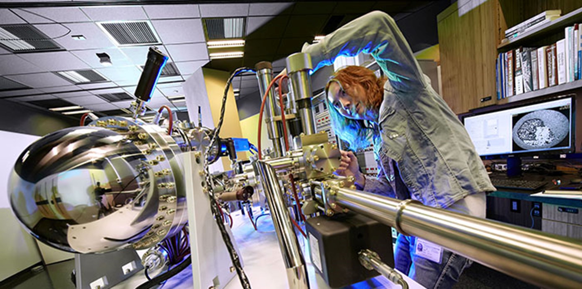
In the microscopy lab, we have pioneered in the development of time-resolved photoemission electron microscopy (TR-PEEM), by combining time resolution of ultrafast optical technique with spatial resolution provided by an electron microscope, we study carrier dynamics at the fundamental time and length scale in semiconductor and photovoltaic materials. This lab is centered around an aberration corrected spectroscopic photoelectron and low energy electron microscope (AC-SPELEEM), which allows imaging of electronic, chemical structure at surfaces and buried interfaces with nanometer spatial resolution. In the last few years, we have utilized our TR-PEEM technique to understand the charge trapping mechanism and the roles of defect in hybrid perovskite photovoltaic materials [1-4], in the studies of 2D material properties [5] and in the manipulation of photocarriers in semiconductors [6].
- [1] T.A.S. Doherty et al., Nature 580, 360 (2020)
- [2] S. Kosar et al., Energy Environ. Sci. 14, 6320-6328 (2021)
- [3] K. Frohna et al., Nat. Nanotechnol. 17, 190-196 (2022)
- [4] S. Macpherson et al., Nature 607, 294-300 (2022)
- [5] M. Rumo et al., Phys. Rev. B 101, 235120 (2020)
- [6] E L. Wong et al., Science Advances 4, eaat9722 (2018)
MAJOR EQUIPMENT
- Elmitec Aberration corrected-SPELEEM (AC-SPELEEM III)
- spatial resolution <8nm, energy resolution <200meV, sample temperature 100-1800K
- Spectra Physics MaiTai HP (690-1020 nm, 80 MHz, 30 nJ, 100 fs)
- Spectra Physics Spirit 1030-140 (1030nm, 0 – 30MHz, 600 µJ < 1Mhz to 150W >1MHz, <400 fs)
- Spectra Physics Spirit NOPA (210 nm to 2500 nm)
- Biophotonics Solutions MIIPSbox640, phase, amplitude and polarization pulse shaper
- Inert Lab 2GB Glovebox
EXPERIMENTAL SETUPS
- THz-time domain spectroscopy
- Pump-probe spectroscopy
- Optical pump- THz probe
- High-harmonic generation setup
- Time-resolved photoemission electron microscopy
- Inert gas glovebox for preparation of samples