FY2017 Annual Report
Femtosecond Spectroscopy Unit
Associate Professor Keshav Dani

Abstract
In recent years, the ability to synthesize, engineer & observe low dimensional materials, with properties determined by variations on the nanometer length scale, has led to novel phenomena and applications. On the other hand, modern lasers deliver powerful, ultrashort pulses of light allowing us to observe the interaction of electrons and atoms on the femtosecond timescale. Together, these technologies allow us to study new paradigms in light-matter interaction – with femtosecond temporal resolution and nanometer spatial resolution. In FY2017, Femtosecond Spectroscopy Unit has directed these abilities and made progress towards three different areas of study:
(a) Low-dimensional materials, where we search for new functionality in materials with applications in optics, electronics and energy;
(b) Terahertz devices & applications, where we investigate the generation of broadband THz radiation and applying this to a variety of materials and devices;
(c) Quantum and Topological Materials, where we study and search for new phenomena at ultrafast timescales in correlated and topological materials.
1. Staff
- Dr. Keshav M. Dani, Professor
- Dr. Michael K. L. Man, Researcher
- Dr. Bala Murali Krishna, Researcher
- Dr. Julien Madéo, Researcher
- Dr. Christopher Petoukhoff, Researcher
- E Laine Wong, Graduate Student
- Viktoras Lisicovas, Graduate Student
- Andrew Winchester, Graduate Student
- Vivek Pareek, Graduate Student
- Joel Pérez Urquizo, Graduate Student
- Yumi Ito, Administrative Assistant
2. Collaborations
Theme: Low-dimensional materials
- Type of collaboration: Joint research
- Researchers:
- Rico Pohle, Okinawa Inst. Of Science and Tech., Japan
- Professor Nic Shannon, Okinawa Inst. Of Science and Tech., Japan
Theme: Terahertz Devices and Applications
- Type of collaboration: Joint research
- Researchers:
- Professor C. Sirtori, Universite Paris Diderot, Paris, France
- Dr. Y. Todorov, Universite Paris Diderot, Paris, France
Theme: Quantum and Topological Materials
- Type of collaboration: Joint research
- Researchers:
- Shukai Yu, Tulane University, USA
- B Gao, Rutgers University, USA
- J.W. Kim, Rutgers University, USA
- S.-W. Cheong, Rutgers University, USA
- D. Talbayev, Tulane University, USA
- C.P. Weber, Santa Clara University, USA
- M. G. Masten, Santa Clara University, USA
- T. C. Ogloza, Santa Clara University, USA
- L. Zhao, Inst. Of Physics & Beijing Laboratory for CMP
- G. Chen, Inst. Of Physics & Beijing Laboratory for CMP, China
- J. Liu, Tulane University, USA
- Z. Mao, Tulane University, USA
- L. M. Schoop, Max Planck Inst. For Solid State Research, Germany
- B. V. Lotsch, Ludwig-Maximilians-Universitat, Germany
- S. S. P. Parkin, Max Planck Inst. Of Microstructure Physics, Germany
- M. Ali, Max Planck Inst. Of Microstructure Physics, Germany
- C. Dhanasekhar, Indian Institute of Technology, Kharagpur, India
- V. Adyam, Indian Institute of Technology, Kharagpur, India
3. Activities and Findings
3.1 Low-dimensional materials
A. Symmetry and optical selection rules in graphene quantum dots
[Physical Review B 97,115404 (2018)]
Nanoscale islands of graphene, also known as graphene quantum dots (GQDs) have attracted a lot of attention over the past years both for their potential applications and for better understanding the effect of confinement on graphene's unique properties. One such feature of graphene is the large, almost constant optical response over a large range of frequencies including the visible spectrum [1]. GQDs, on the other hand, can be viewed as large carbon molecules with a discrete energy spectrum that depends on the size, shape and edge structure of each dot, which results in very different, dot-dependent optical properties [2]. This possibility to engineer their properties based on their geometry is promising for a variety of technological applications, like in solar cells and photo-transistors [3,4]. However, tailoring their properties to a specific application requires the ability to fabricate dots with a specific geometry or to post-select dots with a specific shape or size. Despite recent advances in manufacturing techniques [see e.g. 5-7], complete control over the shape, size and edge geometry has not been achieved yet. Moreover, theoretical work on the optical properties of GQDs has shown interesting effects, like signatures of edge states [8], and edge dependent optical selction rules in triangular dots [9], but a more systematic study over the connection between their geometry and optical properties is still lacking.
In this work, we study the role of size, shape and edge geometry of GQDs on their optical conductivity and derive optical selection rules based on the symmetry of each dot, using group theory. We show that dots with different point-group symmetries have different optical selection rules. In particular, we find that dots with symmetry such as the in-plane (x,y) components of the current operator transform under the same irreducible representation (irreps), the optical conductivity does not depend on the polarization of the incident light (e.g. in triangular and hexagonal dots). On the other hand, dots in which the current operator components transform under different irreps (e.g. in rectangular dots) exhibit a polarization-dependent optical conductivity. We use a simple tight-binding model to illustrate these results with numerical calculations. We also explore how the optical conductivity of GQDs evolve into that of graphene as the size increases. We find that dots with zigzag edges and intermediate size (linear dimension L > 10 nm) exhibit an additional feature in the visible spectrum, absent in dots with armchair edges, which allows the differentiation between dots of different edge geometry. Moreover, we identify a highly degenerate set of electronic states in all types of GQDs that result in a strong peak in the optical conductivity in the ultraviolet and evolves into a similar feature in graphene. Finally we explore the role of asymmetry and disorder (in the form of vacancies) in the optical properties of GQDs. Asymmetry results in a polarization-dependent optical conductivity for each individual dot, although polarization-independence is restored when averaging over an ensemble of dots. On the other hand, the presence of vacancies results in additional features in the optical conductivity, similar to that of dots with zigzag edges.
References Section 3.1 A:
[1] T. Stauber, et al., Phys. Rev. B 78, 085432 (2008).
[2] A. D. Güçlü, et al., Graphene Quantum Dots (Springer, Berlin, 2014).
[3] Quantum Dot Solar Cells, vol. 15, edited by Z. M. W. Jiang Wu (Springer, New York, 2014).
[4] G. Konstantatos, et al., Nat. Nanotechnol. 7, 363 (2012).
[5] L. Wang, et al., Nat. Commun. 5, 5357 (2014).
[6] K. Müllen, ACS Nano 8, 6531 (2014).
[7] M. Olle, et al., Nano Lett. 12, 4431 (2012).
[8] T. Yamamoto, et al., Phys. Rev. B 74, 121409 (2006).
[9] J. Akola, et al., Phys. Rev. B 77, 193410 (2008).
3.2 Terahertz Devices and Applications
A. Engineering the losses and beam divergence in arrays of patch antenna microcavities for terahertz sources
[Journal of Infrared, Millimeter, and Terahertz Waves 38, pp1321-1330 (2017)]
The use of metal-dielectric-metal structures has proven to be an efficient way to confine a terahertz (THz) frequency electromagnetic field into a subwavelength volume. This has led to the realization of high output power THz quantum cascade lasers but at the cost of a poor beam quality and so requiring the use of additional optics [1]. Many designs have been investigated that demonstrate high output powers combined with low beam divergence such as DFB [2], horn antennas [3] and antenna coupled microcavities [4]. In this context, we study the emission from patch antenna microcavities allowing both deep subwavelength confinement (<10-5 λ3) and surface emission. A patch microcavity is a square-shaped resonator that confines the electromagnetic field into a dielectric layer sandwiched by two metallic layers. The resonant frequency of the cavity mode is set by making the top metallic layer of length s= λ/2neff, where neff is the mode index (see Fig. 1 (a)). The use of these structures as emitters yields very divergent radiated beams (see Fig. 1) as well as low photon extraction efficiencies due to low radiative losses [5]. However, arrays of these structures can be adopted to overcome these limitations.

In this work, we present a study on the emission properties of finite arrays of patch-antenna microcavities emitting around 4.5 THz. We investigate the total losses, the radiative and non-radiative contributions to the losses and the far-field radiation pattern, as a function of the geometric parameters of the array. With our simulations, we can extract both the radiative and non-radiative contributions to the total losses and show that it is possible to tune the geometric parameters of the array to have a total control over the losses. Three different regimes are identified: a radiative regime (dominated by the radiative losses), a non-radiative regime (where the metallic losses dominate), and a balanced regime. Fig 2(a) corresponds to the latter case. We can see that for a distance between resonators of d=40 µm, a perfect balance between the radiative and non-radiative losses can be achieved, leading to higher quality factors. We also show the possibility to engineer the far-field pattern of the array by designing a far-field interference. By adjusting the number and position of the microcavity resonators, small divergence angles can be obtained (see Fig. 2(b)). Fig. 2 (c) summarizes the photon extraction efficiencies for N= 10 resonators (calculated as Q/Qrad) as a function of the spacing between the resonators. For L=5 µm, extraction efficiencies larger than 90% are calculated. These results are consistent with our previous work where optimized quality factors were obtained with similar geometric parameters, achieving high Purcell factors in the structure leading to enhanced electroluminescence [6]. In conclusion, arrays of patch-antenna microcavities allow a precise tuning of the losses, leading to high extraction efficiencies and the shaping of the beam. This structure can pave the way to realizing efficient THz emitters and provide an alternative way to achieve phased locked laser arrays and THz amplifiers.

References Section 3.2 A:
[1] B. S. Williams, Nature Photonics 1, 517-525 (2007).
[2] M. I. Amanti et al., Nature Photonics 3, 586-590 (2009).
[3] F. Wang et al. Optics Express 24, 2174-2182 (2016).
[4] T.-Y. Kao et al.Nature Photonics 10, 541-546 (2016).
[5] C. Feuillet-Palma et al., Scientific Reports 3, 1361 (2013).
[6] J. Madéo et al., Appl. Phys. Lett. 109, 141103 (2016).
3.3 Quantum and Topological Materials
A. High-Temperature Terahertz Optical Diode Effect without Magnetic Order in Polar FeZnMo3O8
[Physics Review Letters 120,037601 (2018)]
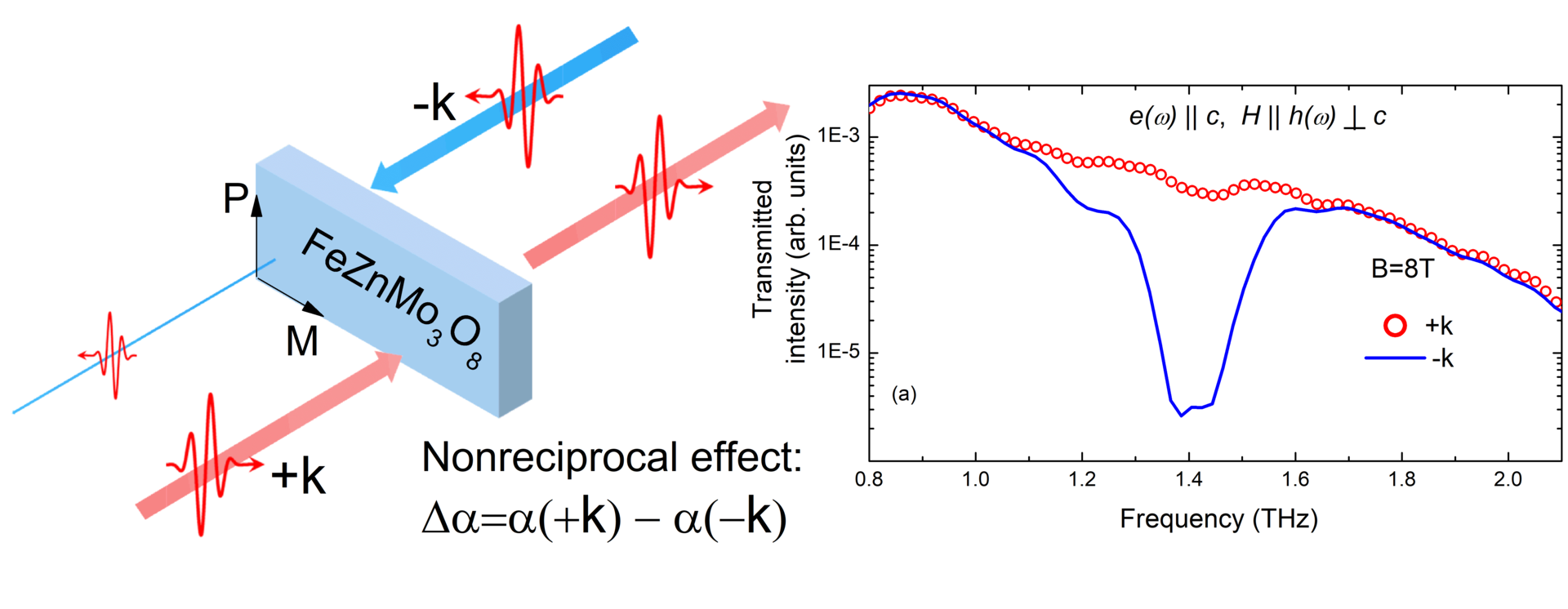
Multiferroic materials that exhibit simultaneous magnetic and ferroelectric orders have been the source of many fascinating phenomena and functionalities. One of interesting phenomena is terahertz (THz) optical diode effect (ODE), or THz nonreciprocal directional dichroism, which has potential application in THz optical isolator [1,2]. Nonreciprocal directional dichroism is defined as difference in the absorption coefficient for linearly polarized light traveling in the opposite direction (Fig. 3). Practical devices require the display of effect intense and close to room temperature. However, most of the reported nonreciprocal directional dichroism observations until now happened in low temperature magnetically ordered states [3,4]. Room temperature ferroelectric antiferromagnetic ordered BiFeO3 has ODE, but its magnitude is rather small [3]. Discovery the materials that have high temperature and strong ODE become critical in practical application.
In this work, we reported the observation of giant high temperature THz ODE in polar ferrimagnetic FeZnMo3O8. We observed that the transmitted light intensity in one direction is over 100 times lower than intensity transmitted in the opposite direction. Most remarkably, the strong ODE persists in the high-temperature paramagnetic state of FeZnMo3O8 without long-range magnetic order up to 110 K, which is in stark contrast with all previous reports of THz ODE where the presence of magnetic order is a necessity. In FeZnMo3O8, the effect occurs resonantly with a strong magnetic dipole active transition centered at 1.27 THz and assigned as electron spin resonance between the eigenstates of the single-ion anisotropy Hamiltonian. We propose that the optical diode effect in paramagnetic FeZnMo3O8 is driven by single-ion terms in magnetoelectric free energy.
References Section 3.3 A:
[1] S.-W. Cheong, et al., Nature Materials 6, 13 (2007).
[2] R. Ramesh, et al., Nature Materials 6, 21 (2007).
[3] I. Kézsmárki, et al., Physics Review Letters, 106, 057403 (2011).
[4] R. Masuda, et al., Physics Review B, 96, 041117(R) (2017).
[5] I. Kézsmárki, et al., Physics Review Letters, 115, 127203 (2015).
B. Terahertz-frequency magnetoelectric effect in Ni-doped CaBaCo4O7
[Physics Review B 96, 094421 (2017)]
CaBaCo4O7 (CBCO) is a class of magnetoelectric multiferroic materials where magnetic order and electric polarization are strong coupled. Strong magnetoelectricity has been reported in CBCO as it enters the ferrimagnetic phase with Tc ~ 60 K: A large polarization change ΔP = 17 mC/m2 happens due to the magnetic ordering [1]. The magnetically induced polarization change is much higher than the one reported in magnetic improper ferroelectrics GdMn2O5 with value of magnetically tuned polarization change [5] of ΔP = 5 mC/m2 . Magnetoelectricity can potentially be useful in sensors, actuators, or data-storage applications. Thus, a detailed microscopic understanding of this effect is necessary.
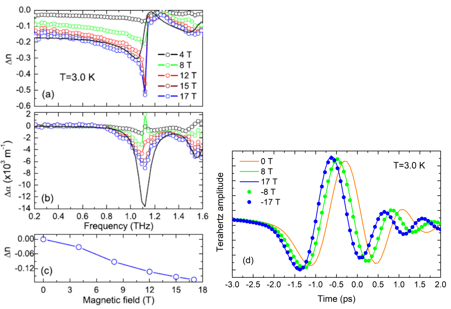
In this work, we observed the magnetoelectric effect of Ni-doped CBCO in terahertz (THz) frequency range. Terahertz refractive index and absorption are changed by the magnetic fields up to 17 T (Fig. 4). The magnetic field modulates the strength of infrared-active optical phonons near 1.2 and 1.6 THz. Lorentz model of the dielectric function is employed to analyze the measured magnetic-field dependence of the refractive index and absorption. The results show that most of the magnetoelectric effect is contributed by the optical phonons near 1.6 THz and higher frequency resonances. Our experimental results can be used to construct and validate more detailed theoretical descriptions of magnetoelectricity in CaBaCo4−xNixO7.
References Section 3.3 B:
[1] V. Caignaert, et al., Physics Review B 88, 174403 (2013).
[2] N. Lee, et al., Physics Review Letters 110, 137203 Number (2013).
C. Similar ultrafast dynamics of several dissimilar Dirac and Weyl semimetals
[Journal of Applied Physics 122, 223102 (2017)]
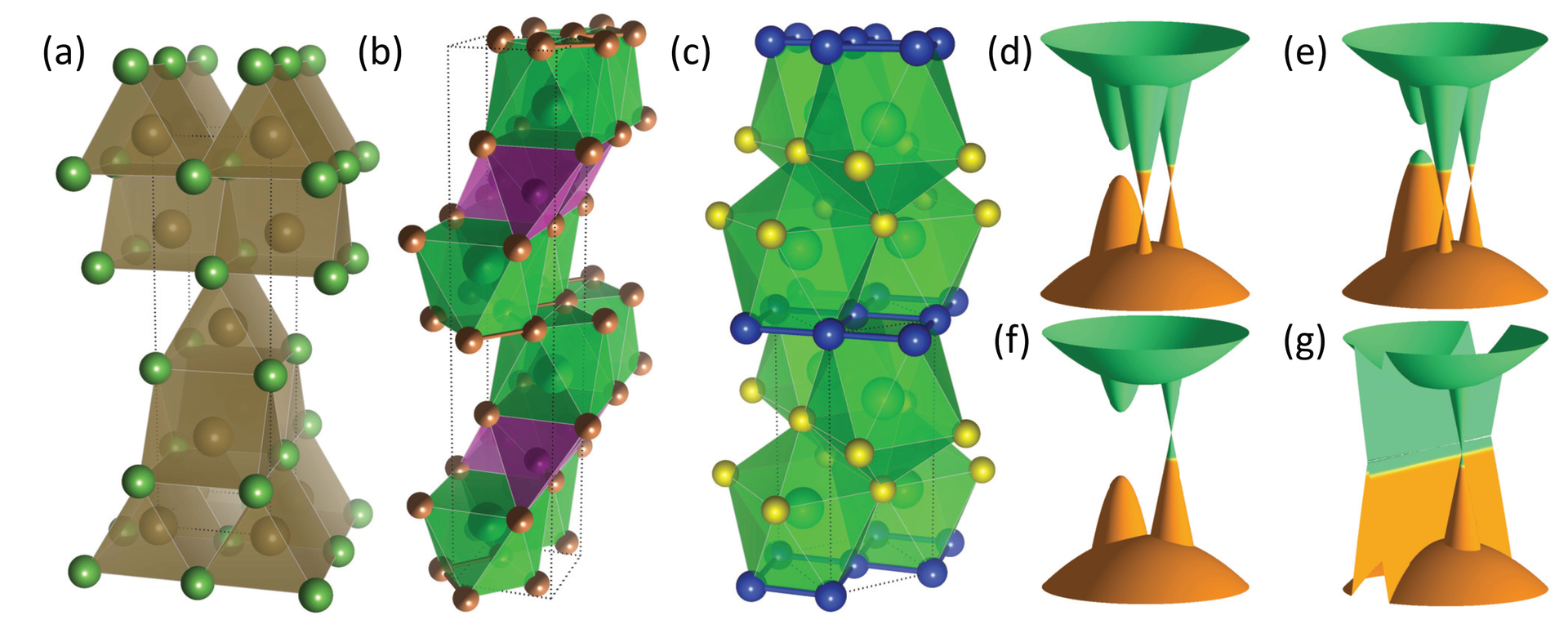
Recent years have seen the rapid discovery of solids whose low-energy electrons have a massless, linear dispersion, such as Weyl [1], line-node [2], and Dirac semimetals [3]. The remarkable optical properties predicted in these materials show their versatile potential for optoelectronic uses. However, little is known of their response in the picoseconds after absorbing a photon and knowledge of material’s sub- and few-picosecond response to optical excitation reveals, for instance, the properties of hot electrons important in high-field devices. Here, we measure the ultrafast dynamics of four materials that share non-trivial band structure topology but that differ chemically, structurally, and in their low-energy band structures (see Fig.5): ZrSiS, which hosts a Dirac line node and Dirac points; TaAs and NbP, which are Weyl semimetals; and Sr1–yMn1–zSb2, in which Dirac fermions coexist with broken time-reversal symmetry.
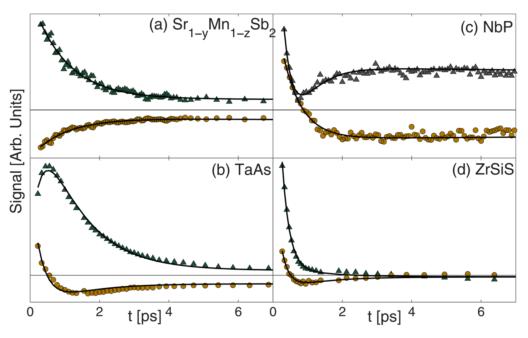
After photoexcitation by a short pulse, all four relax in two stages, first sub-picosecond and then few-picosecond. Their rapid relaxation suggests that these and related materials may be suited for optical switches and fast infrared detectors. The complex change of refractive index shows that photoexcited carrier populations persist for a few picoseconds (see Fig.6).
As new Dirac and Weyl semimetals are discovered, whether in the same material families as our samples or in new ones, they will all share the linear dispersion and low density of states near the Fermi energy that dictate the ultrafast properties of our samples. Thus, we can anticipate a rapid, two-part ultrafast response, similar to the one that makes the four materials we have studied promising for optoelectronic applications such as terahertz detectors or saturable absorbers. This ultrafast response could be especially useful if combined with the materials’ demonstrated large, anisotropic, optical nonlinearity, [4] or with any of the materials’ remarkable predicted optical properties [5-7].
References Section 3.3 C:
[1] X. Wan, et al., Phys. Rev. B 83, 205101 (2011).
[2] A. A. Burkov, et al., Phys. Rev. B 84, 235126 (2011).
[3] S. M. Young, et al., Phys. Rev. Lett. 108, 140405 (2012).
[4] L. Wu, et al., Nature Physics 13, 350 (2017).
[5] C.-K. Chan, et al., Phys. Rev. B 95, 041104 (2017).
[6] J. M. Shao, et al., AIP Adv. 5, 117213 (2015).
[7] Y. Baum, et al., Phys. Rev. X 5, 041046 (2015).
4. Publications
4.1 Journals
- R. Pohle, E. G. Kavousanaki, K. M. Dani, and N. Shannon, Symmetry and optical selection rules in graphene quantum dots, Phys. Rev. B 97, 115404 (2018).
- S. Yu, B. Gao, J. W. Kim, S.-W. Cheong, M. K. L. Man, J. Madéo, K. M. Dani, and D. Talbayev, High-temperature terahertz optical diode effect without magnetic order in polar FeZnMo3O8, Phys. Rev. Lett. 120, 037601 (2018).
- C. P. Weber, B. S. Berggren, M. G. Masten, T. C. Ogloza, S. Deckoff-Jones, J. Madéo, M. K. L. Man, K. M. Dani, L. Zhao, G. Chen, J. Liu, Z. Mao, L. M. Schoop, B. V. Lotsch, S. S. P. Parkin, and M. Ali, Similar ultrafast dynamics of several dissimilar Dirac and Weyl semimetals, J. Appl. Phys. 122, 223102 (2017).
- S. Yu, C. Dhanasekhar, V. Adyam, S. Deckoff-Jones, M. K. L. Man, J. Madéo, E L. Wong, T. Harada, M. B. M. Krishna, K. M. Dani, and D. Talbayev, Terahertz-frequency magnetoelectric effect in Ni-doped CaBaCo4O7, Phys. Rev. B 96, 094421 (2017).
- J. Madéo, J. Pérez-Urquizo, Y. Todorov, C. Sirtori, and K. M. Dani, Engineering the losses and beam divergence in arrays of patch antenna microcavities for terahertz sources, J. Infrared Milli. Terahz. Waves (2017). doi:10.1007/s10762-017-0418-6.
4.2 Books and Other One-Time Publications
Nothing to report.
4.3 Oral and Poster Presentations
- Madeo, J., Todorov, Y., Perez-Urquizo, J., Gilman, A., Frucci, G., Li, L., Davies, A. G., Linfield, E. H., Carlo, S., Dani, K. M., Antenna-coupled microcavities for terahertz emission, Invited Talk, EMN Optoelectronics 2017, Victoria, Canada, Apr 18-21 (2017)
- Man, M. K. L., Imaging electron motions in 2D semiconductor heterojunctions, Invited Talk, 2017 Joint APS/CNN User Meeting, Chicago, USA, May 8-11 (2017)
- Man, M. K. L., Margiolakis, A., Deckoff-Jones, S., Harada, T., Wong, E., Mariserla, B. M. K., Madeo, J., Winchester, A., Lei, S., Vajtai, P. M., Ajayan, P. M., Dani, K. M., Imaging electron motions in 2D semiconductor heterojunctions, Oral Presentation, CLEO2017, San Jose, CA, USA May 13-18 (2017)
- Petoukhoff, C. E., Mariselra, B. M. K., Voiry, D., Bozkurt, I., Deckoff-Jones, S., Chhowalla, M., O’Carroll, D. M., Dani, K. M., Charge Transfer and Enhanced Absorption in MoS2 - Organic Heterojunctions Using Plasmonic Metasurfaces, Poster Presentation, CLEO2017, San Jose, CA, USA May 13-18 (2017)
- Winchester, A., Wong, E., Man, M. K. L., Pareek, V., Madeo, J., Dani, K. M., Exploring Ultrafast Electron Dynamics in Space, Time, Momentum and Energy, Oral Presentation, CLEO2017, San Jose, CA, USA May 13-18 (2017)
- Wong, E., Winchester A., Man, M. K. L., Pareek, V., Madeo, J., Dani, K. M., Imaging complex electron dynamics within a photoexcitation spot, Oral Presentation, CLEO2017, San Jose, CA, USA May 13-18 (2017)
- Madeo, J., Exploring the ultrafast dynamics of 2D semiconductors with high spatial resolution, Invited Talk, CCMR2017, Jeju, South Korea, Jun 26-30 (2017)
- Man, M. K. L., Exploring new dimensions in ultrafast electron dynamics with time-resolved photoemission electron microscopy, Poster Presentation, International workshop on strong correlations and angle-resolved photoemission spectroscopy 2017, Hiroshima, Japan, Jul 2-7 (2017)
- Dani, K. M., Cinematography of Charge: The Art of Making Movies of Electrons, Invited Talk, EDISON 20, Buffalo, NY USA, Jul 16-21 (2017)
- Dani, K. M., Cinematography of Charge; The Art of Making Movies of Electrons, Invited Talk, Student Research Symposium: Reflections of Life at the Forefront of Nanotechnology, Buffalo, NY USA, Jul 22 (2017)
- Dani, K. M., Imaging the dynamics of photoexcited electrons in a type-II semiconductor heterostructure, Invited Talk, CLEO PR OECC PGC, Singapore, Jul 31- Aug 4 (2017)
- Petoukhoff, C., Mariserla, B. M. K., Bozkurt, I., Chhowalla, M., O’Carroll, D. M., Dani, K. M., Ultrafast Charge Transfer in Mixed-Dimensional van der Waals Heterostructures, Poster Presentation, IONS Okinawa 2017, Okinawa, Japan Oct 25-27 (2017)
- Man, M. K. L, Imaging Electron Motions in 2D Semiconductor Heterojunctions, Invited Talk, International Workshop on PEEM and its Applications, Beijing, China, Nov 22-25 (2017)
- Petoukhoff, C., Mariserla, B. M. K., Bozkurt, I., Chhowalla, M., O’Carroll, D. M., Dani, K. M., Charge Transfer in Conjugated Polymer, MoS2 – Metasurface Mixed – Dimensional Heterojunctions, Poster Presentation, MRS Fall 2017, Boston, MA, USA, Nov 26- Dec 1 (2017)
- Dani, K. M., Cinematography of Charge- Making Movies of Electrons in Motion in 2D Semiconductors, Invited Talk, MRS Fall 2017, Boston, MA, USA, Nov 26- Dec 1 (2017)
- Vivek, P., Berggren, B. S., Harada, T., Weber, C. P., Winchester, A., Mariserla, B. M. K., Madeo, J., Dani, K. M., Ultrafast carrier dynamics in atomically thin black phosphorus, Poster Presentation, ICANN 2017, Guwahati, India, Dec 18-21 (2017)
- Dani, K. M., Man, K. L., Margiolakis, A., Deckoff-Jones, S., Harada, T., Wong, E., Mariserla, B. M. K., Madeo, J., Winchester, A., Lei, S., Vajtai, R., Ajayan, P. M., Time-resolved photomission electron microscopy of a type-II semiconductor heterojunction, Invited Talk, ICANN 2017, Guwahati, India, Dec 18-21 (2017)
- Dani, K. M., Cinematography of Charge- the art of making movies of photoexcited electrons in materials, Invited Talk, ISEST 2018, OIST, Okinawa, Japan, Jan 22-26 (2018)
- Pareek, V., Berggren, B., Harada, T., Weber, C., Winchester, A., Mariserla, B. M. K., Madeo, J., Dani, K. M., Ultrafast dynamics in atomically thin black phosphorus, APS March Meeting 2018, Los Angeles, CA, USA, Mar 5-9 (2018)
- Pérez-Urquizo, J., Madeo, J., Todorov, Y., Sirtori, C., Dani, K. M., Patch antenna microcavity arrays for THz sources, APS March Meeting 2018, Los Angeles, CA, USA, Mar 5-9 (2018)
- Winchester A., Petoukhoff, C., Adbi-Jalebi, M., Andaji-Garmaroudi, Z., Pareek, V., Wong, E., Madeo, J., Man, M. K. L., Stranks, S., Dani, K. M., Investigation of local nanoscale electronic variation and photo excited carrier dynamics in hybrid organic-inorganic mixed cation perovskite films, Oral Presentation, APS March Meeting 2018, Los Angeles, CA, USA, Mar 5-9 (2018)
- Wong, E., Winchester, A., Man, M. K. L., Pareek, V., Madeo, J., Dani, K. M., Controlling the vertical transport of photocarriers to the surface, Oral Presentation, APS March Meeting 2018, Los Angeles, CA, USA, Mar 5-9 (2018)
5. Intellectual Property Rights and Other Specific Achievements
Nothing to report.
6. Meetings and Events
6.1 Seminar
- Date: Jun 2nd 2017
- Venue: C700, OIST Campus
- Speaker: Chris Nicholson
- Date: Aug 25th 2017
- Venue: B503 OIST Campus
- Speaker: Dr. Carolina Rendon
- Date: Sep 26th 2017
- Venue: C210 OIST Campus
- Speaker: Dr. Edmund Kelleher
- Date: Oct 5th and 6th 2017
- Venue: C210/C700, OIST Campus
- Speaker: Prof. Yann Gallais
- Date: Nov 10th 2017
- Venue: C016 OIST Campus
- Speaker: Shunya Maezawa
6.2 Workshop
Nothing to report.
7. Others
Nothing to report.


