

LEEM / PEEM (pre 170905)
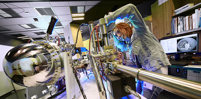
In the Femtosecond Spectroscopy Unit, we aim to combine time resolution of ultrafast optical technique with spatial resolution of an electron microscope to study spatially resolved ultrafast electronics processes at the femtosecond timescale. For this purpose, our unit is equipped with a low-energy/photo-emission electron microscope (LEEM/PEEM) and several high power femtosecond lasers. LEEM/PEEM is a powerful and versatile technique that utilizes a range of complementary analysis methods to characterize 2D materials, inhomogeneous surfaces, ultrathin films and buried interfaces. To enable visualization of ultrafast dynamic processes, such as charge carrier dynamics during photo-excitation or spin dynamics in magnetic nanomaterials, we use photo-emitted electrons generated by a femtosecond laser to provide time resolution at ultrafast timescale, and meanwhile the electron microscope with give us spatial resolution at the nanometer range. Spatial visualization of the electronics dynamic processes at their fundamental time and length scale will help advance our understanding in the physics processes behind the emerging nanotechnologies.
Photo Emission Electron Microscopy (PEEM)
PEEM images sample surface with photo-emitted electrons that are generated by UV or x-ray light source. The photo-emitted electrons carry information about the local environment from where they are originated from. Our PEEM is equipped with an imaging energy analyzer, which enable us to perform spatially resolved photoemission spectroscopy (PES/UPS/XPS) with lateral resolution better than 15nm and at energy resolution better than 300meV. This technique provides information such as valence energy levels, and chemical bonding state of the near surface region of the sample. Besides direct imaging of sample surfaces, the microscope can also resolve photo-emitted electrons escaped from the sample at different azimuthal angles and at different energy (Photo-emitted electron diffraction/Angle-resolved Photoemission spectroscopy PED/ARPES). This technique let us study the electronic structure in materials and reconstruct the 3D Fermi surfaces at high spatial resolution.
In our laboratory, several UV light sources are currently available. Surface imaging can be done with a quasi-CW UV laser or an ultrafast pulsed UV laser, while conventional and time-resolved ARPES can be done using a He plasma discharge light source and an ultrafast pulsed extreme UV light source, respectively.

Schematic of the LEEM/PEEM
Low energy electron microscopy (LEEM)
Besides imaging with photo-emitted electron, our microscopy can also work as a LEEM as it is equipped with a conventional electron cathode. LEEM images surfaces with elastically backscattered low energy electrons. Due to large backscattering cross sections of low energy electrons and non-scanning imaging principle of the cathode immersion lens design, LEEM imaging can be carried out routinely in real-time at video frame rate. It is an ideal instrument for monitoring in situ dynamic processes, such as growth and self-organization of nanostructures and thin films. Lateral resolution of the LEEM installed in OIST is better than 10nm. However, with an aberration correction upgrade, resolution better than 2nm is achievable.
In LEEM, imaging is done with two major contrast mechanisms, namely diffraction contrast and phase contrast. For diffraction contrast, bright field imaging is done using backscattered electrons that undergo no momentum transfer parallel to the surface. In this mode, contrast comes from local variation of the structure factor on the sample surface. On the other hand, dark field imaging using diffracted electrons with non-zero parallel momentum transfer is also possible and it is useful in identification of coexisting phases of different rotational variants.
The other contrast mechanism, phase contrast, can be further divided up into geometry phase contrast and quantum size contrast. In geometry phase contrast, the height different of steps on surface give raise to phase different in the backscattered electron wave, interference of these backscattered electron waves lead to amplitude differences and it allows imaging of steps at surfaces. Quantum size contrast is based on interference of electron wave backscattered from the surface and from the thin film/substrate interface, which produce intensity maxima and minima depending on thickness of the thin film and the electron energy. This mechanism allows quantitative measurement of film thickness on surfaces.
Besides direct imaging of surfaces, we can also image the back focal plane of the objective lens which gives access to low energy electron diffraction (LEED). In this mode, structural information from very small selected area as small as 250nm can be obtained by insertion of a small aperture in the electron beam path.
The combination of all the techniques in PEEM and LEEM allows us to investigate chemical, electronics, and structural properties of materials at very high spatial resolution. It is particular useful in the study of nanomaterials or inhomogeneous surfaces such as 2D structures.
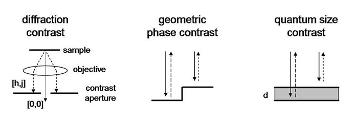
Contrast mechanisms in LEEM
Highlights
- Highest resolution (< 8 nm)
- Operation modes:
- PEEM : Photoemission electron microscopy
- PES/UPS : Photoemission spectroscopy
- μ-ARPES : micro-Angle resolved photoemission spectroscopy (<1µm)
- LEEM : Low energy electron microscopy
- MEM : Mirror energy microscopy
- TEEM : Thermionic emission electron microscopy
- μ-LEED : micro-Low energy electron diffraction (<250nm)
- μ-EELS : micro-Electron energy loss spectroscopy (<250nm)
- UHV in-situ monitoring of dynamic processes such as crystal growth or phase transitions
- Wide sample temperature range (~100 K to 1800 K)
(Installation of the LEEM/PEEM system is completed at the end of February 2013 and setup of the extreme UV light source is done in June 2014.)