

FY2020 Annual Report
Energy Materials and Surface Sciences Unit
Abstract
Halide perovskites have been considered as the “star materials” for scientific research in recent years. Because of the strong optical adsorption, low non-radiative recombination rates, tunable band gaps, relatively high charge-carrier mobility, long diffusion lengths and solution processability, halide perovskites have shown great advantages in photovoltaic applications including solar cells, light-emitting diodes (LEDs) and photodetectors. However, the high sensitivity of halide perovskites to air, humidity and heat severely limits their practical application foregrounds. To solve the stability problem of perovskite solar modules, a holistic approach to interface stabilization was applied by Zonghao Liu et al. to achieve the stable operation over 2000 hours. Besides, this optimized perovskite solar module has high power conversion efficiency (PCE) of 16.6% for a designated area of 22.4 cm2, which is a big step forward to the commercialization of perovskite solar cells. In addition, we developed inorganic perovskite nanowires and micro-nanowire arrays to fabricate high performance photodetectors with long-term operational stability. Furthermore, we expanded our research of halide perovskites to LEDs and realized the highly efficient red and green LEDs by CsPbBrxI3-x and silica network facilitated perovskites.
1. Unit Members
• Ms. Naoko Ogura-Gayler, Research Unit Administrator
• Dr. Luis K. Ono, Group Leader
• Dr. Guoqing Tong, Researcher
• Dr. Hui Zhang, Researcher
• Dr. Yuiqiang Liu, Researcher
• Dr. Tongle Bu
• Ms. Afshan Jamshaid, OIST Graduate Student
2. Collaborations
- Efficient Perovskite LEDs with Tetraethoxysilane (TEOS) Passivation - Nano Energy 78, 105134 (2020).
- Type of collaboration: collaborative research
- Collaborators:
- Prof. Baoquan Sun, Soochow University, China
- Prof. Baoquan Sun, Soochow University, China
- Efficient Perovskite Solar Cells with Photon Up-conversion Strategy - ChemPhotoChem. 4, 5271–5278 (2020).
- Type of collaboration: collaborative research
- Collaborators:
- Prof. Nobuhiro Yanai, Kyushu University, Japan.
- Prof. Nobuo Kimizuka, Kyushu University, Japan.
3. Activities and Findings
3.1 The development of scalable and stable perovskite solar modules.
Zonghao Liu†, Longbin Qiu†, Luis K. Ono, Sisi He, Zhanhao Hu, Maowei Jiang, Guoqing Tong, Zhifang Wu, Yan Jiang, Dae-Yong Son, Yangyang Dang, Said Kazaoui, Yabing Qi*, "A holistic approach to interface stabilization for efficient perovskite solar modules with over 2,000-hour operational stability" Nat Energy 5, 596-604 (2020). († equal contribution).
Longbin Qiu†, Sisi He†, Zonghao Liu, Luis K. Ono, Dae-Yong Son, Yuqiang Liu, Guoqing Tong, Yabing Qi*, "Rapid hybrid chemical vapor deposition for efficient and hysteresis-free perovskite solar modules with an operation lifetime exceeding 800 hours" J. Mater. Chem A 8, 23404 (2020). († equal contribution).
The upscaling of perovskite solar cells to module scale and long-term stability have been recognized as the most important challenges for the commercialization of this emerging photovoltaic technology. In a perovskite solar module, each interface within the device contributes to the efficiency and stability of the module. Here, we employed a holistic interface stabilization strategy by modifying all the relevant layers and interfaces, namely the perovskite layer, charge transporting layers and device encapsulation, to improve the efficiency and stability of perovskite solar modules. The treatments were selected for their compatibility with low-temperature scalable processing and the module scribing steps. Our unencapsulated perovskite solar modules achieved a reverse-scan efficiency of 16.6% for a designated area of 22.4 cm2. The encapsulated perovskite solar modules, which show efficiencies similar to the unencapsulated one, retained approximately 86% of the initial performance after continuous operation for 2,000 h under AM1.5G light illumination, which translates into a T90 lifetime (the time over which the device efficiency reduces to 90% of its initial value) of 1,570 h and an estimated T80 lifetime (the time over which the device efficiency reduces to 80% of its initial value) of 2,680 h.
Hybrid chemical vapor deposition (HCVD) has been employed in the fabrication of perovskite solar cells (PSCs) and modules (PSMs), and it shows strong promise for upscalable fabrication. The conventional HCVD process needs a relatively long processing time (e.g., several hours) and the fabricated PSCs often exhibit salient hysteresis, which impedes utilization of this technology for mass production. Herein, we demonstrate a rapid HCVD (RHCVD) fabrication process for PSCs using a rapid thermal process, which not only significantly reduces the deposition time to less than 10 min, but also effectively suppresses hysteresis. This markedly reduced deposition time is comparable to that of solution-coating processes. Furthermore, the shorter processing time inside the furnace reduces the exposure time of the glass/ITO/SnO2 substrates under vacuum, which helps maintain the high quality of the SnO2 electron-transport layer and results in a lower density of gap states. Finally, PSMs with a designated area of 22.4 cm2 fabricated via RHCVD achieved an efficiency of 12.3%, and maintained 90% of the initial value after operation under continuous light illumination for over 800 h.
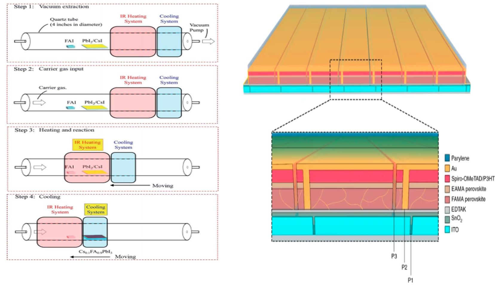
Figure 1: (Left) Hybrid chemical vapor deposition. (Right) Stable perovskite solar module by holistic interface stabilization method.
3.2 The application of inorganic perovskites in photodetectors.
Guoqing Tong, Maowei Jiang, Dae-Yong Son, Luis K. Ono, Yabing Qi*, "2D derivative phase induced growth of 3D all inorganic perovskite micro-nanowire array based photodectors" Adv. Funct. Mater. 2002526 (2020).
Guoqing Tong, Maowei Jiang, Dae-Yong Son, Longbin Qiu, Zonghao Liu, Luis K. Ono, Yabing Qi*, "Inverse growth of large-grain-size and stable inorganic perovskite micronanowire photodetectors" ACS Appl. Mater. Interfaces 12, 14185-14194 (2020).
A large number of derivative phases in inorganic perovskites are reported with special structures and extraordinary performances in photoelectronic device applications. The reverse phase transition between derivative phases and perovskites usually induces recrystallization or forms mixed components. In this work, derivative phase-induced growth of the CsPbBr3 micro–nanowire (MW) array by utilizing phase transition of the 2D CsPb2Br5 phase is reported. Owing to its layered structure and phase transition, annealing of CsPb2Br5 at a temperature of 550 °C combined with solvent quenching leads to a templating effect to form a high-quality CsBr MW array. Subsequent PbBr2 deposition and the second annealing are employed to form aligned CsPbBr3 MW arrays. Based on this method, a CsPbBr3 MW array-based photodetector is fabricated. The large grain size, less grain boundaries, and lower surface potential of the CsPbBr3 MW array lead to high device performance with a responsivity of 7.66 A W−1 , a detectivity of ≈1012 Jones, and long-term operational stability over 1900 min.
Control of forward and inverse reactions between perovskites and precursor materials is key to attaining high-quality perovskite materials. Many techniques focus on synthesizing nanostructured CsPbX3 materials (e.g., nanowires) via a forward reaction (CsX + PbX2 → CsPbX3). However, low solubility of inorganic perovskites and complex phase transition make it difficult to realize the precise control of composition and length of nanowires using the conventional forward approach. Herein, we report the self-assembly inverse growth of CsPbBr3 micronanowires (MWs) (CsPb2Br5 → CsPbBr3 + PbBr2↑) by controlling phase transition from CsPb2Br5 to CsPbBr3. The two dimensional (2D) structure of CsPb2Br5 serves as nucleation sites to induce initial CsPbBr3 MW growth. Also, phase transition allows crystal rearrangement and slows down crystal growth, which facilitates the MW growth of CsPbBr3 crystals along the 2D planes of CsPb2Br5. A CsPbBr3 MW photodetector constructed based on the inverse growth shows a high responsivity of 6.44 A W−1 and detectivity of ∼1012 Jones. Large grain size, high crystallinity, and large thickness can effectively alleviate decomposition/degradation of perovskites, which leads to storage stability for over 60 days in humid environment (relative humidity = 45%) and operational stability for over 3000 min under illumination (wavelength = 400 nm, light intensity = 20.06 mW cm−2).
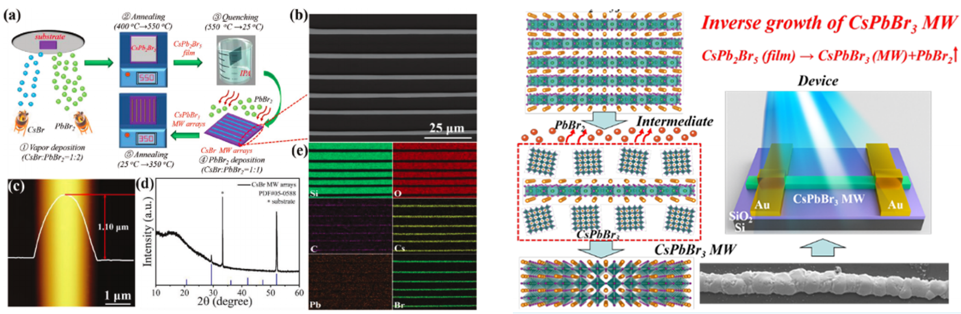
Figure 2: Application of inorganic perovskite in photodetecors.
3.3 Exploration of perovskite materials in light-emitting diodes (LEDs).
Maowei Jiang, Zhanhao Hu, Luis K. Ono, Yabing Qi*, "CsPbBrxI3-x thin films with multiple ammonium ligands for low turn-on pure-red perovskite light-emitting diodes" Nano Research 14, 191-197 (2020).
Yuqiang Liu, Lei Cai, Yafeng Xu, Junnan Li, Yuanshuai Qin, Tao Song, Lu Wang, Youyong Li, Luis K. Ono, Yabing Qi*, Baoquan Sun*, "In-situ passivation perovskite targeting efficient light-emitting diodes via spontaneously formed silica network" Nano Energy 78, 105134 (2020).
All-inorganic α-CsPbBrxI3-x perovskites featuring nano-sized crystallites show great potential for pure-red light-emitting diode (LED) applications. Currently, the CsPbBrxI3–x LEDs based on nano-sized α-CsPbBrxI3-x crystallites have been fabricated mainly via the classical colloidal route including a tedious procedure of nanocrystal synthesis, purification, ligand or anion exchange, film casting, etc. With the usually adopted conventional LED device structure, only high turn-on voltages (> 2.7) have been achieved for CsPbBrxI3-x LEDs. Moreover, this mix-halide system may suffer from severe spectra-shift under bias. In this report, CsPbBrxI3-x thin films featuring nano-sized crystallites are prepared by incorporating multiple ammonium ligands in a one-step spin-coating route. The multiple ammonium ligands constrain the growth of CsPbBrxI3-x nanograins. Such CsPbBrxI3-x thin films benefit from quantum confinement. The corresponding CsPbBrxI3-x LEDs, adopting a conventional LED structure of indium-doped tin oxide (ITO)/poly(3,4-ethylenedioxythiophene):poly(styrenesulfonate) (PEDOT:PSS)/CsPbBrxI3-x/[6, 6]-phenyl C61 butyric acid methyl ester (PCBM)/bathocuproine (BCP)/Al, emit pure-red color at Commission Internationale de l’éclairage (CIE) coordinates of (0.709, 0.290), (0.711, 0.289), etc., which represent the highest color-purity for reported pure-red perovskite LEDs and meet the Rec. 2020 requirement at CIE (0.708, 0.292) very well. The CsPbBrxI3-x LED shows a low turn-on voltage of 1.6 V, maximum external quantum efficiency of 8.94%, high luminance of 2,859 cdm−2, and good color stability under bias.
Perovskite materials are attractive candidates as emitting layers in light-emitting diodes due to their excellent optical and electrical properties. Effective charge radiative recombination is a key to target high-efficiency perovskite light-emitting diodes (PeLEDs). State-of-the-art effective passivation chemicals in PeLEDs mostly belong to organic chelating molecules, associated with like molecular detachment in the device operation, which simultaneously degrades the performance especially the operational stability of the devices. Here, a silane material tetraethoxysilane (TEOS), which can be crosslinkable to avoid any likely detachment from perovskite film, is incorporated into the perovskite film to enhance film radiative recombination and stability. An oxo-bridged silica network anchored with perovskite is formed after the TEOS in-situ crosslinking process. It is found that the lone pair electrons in TEOS network can coordinate with the undercoordinated Pb2+ of perovskite. Consequently, defect states in perovskite film are dramatically diminished, which enhances radiative recombination. The photoluminescence intensity of resultant perovskite-TEOS film is enhanced by 40% over that of the pristine one. The average photoluminescence lifetime of perovskite-TEOS film reaches 58 ns, enhanced by 65% over that of the pristine perovskite film of 35 ns. As a result, a green PeLED achieved an external quantum efficiency of 16.6% with improved working stability. This work presents a facile strategy targeting efficient and stable perovskite devices via utilizing detachment-free self-crosslinked ligands
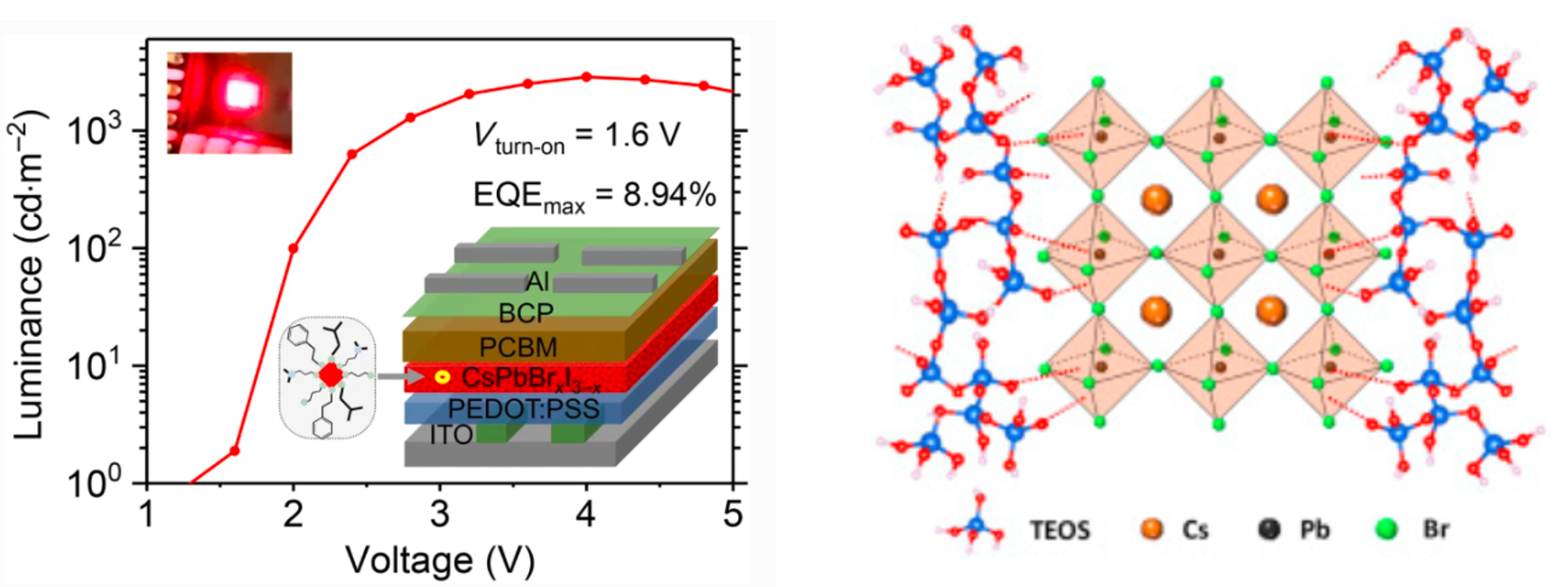
Figure 3: Application of perovskite in light-emitting diodes (LEDs).
4. Publications
4.1 Journals
→Please see our publications page for published journals
4.2 Books and Other One-Time Publications
N/A
4.3 Oral and Poster Presentations
- Yabing Qi, "Surface science in perovskite solar cells", Science China Materials Online International Conference, July 19, 2020. (Invited talk).
- Yabing Qi, "Perovskite solar cells", Webinar on "Carbon Negative Technology Innovations Fighting Climate Change" organized by The PICHIR Climate Adaption Collective Team and OIST Foundation, February 11, 2021. (Invited seminar).
5. Intellectual Property Rights and Other Specific Achievements
N/A
6. Meetings and Events
1 Y. B. Qi, “Surface Science in Perovskite Solar Cells”, Science China Materials Online International Conference (July 19, 2020) (Invited talk).
2 Y. B. Qi, “Perovskite Solar Cells”, Webinar on “Carbon Negative Technology Innovations Fighting Climate Change” organized by The PICHTR Climate Adaptation Collective Team and OIST Foundation (February 11, 2021) (Invited seminar).