

FY2014 Annual Report
Energy Materials and Surface Sciences Unit
Abstract
Currently, more than 80% of the world’s energy generation is originated from fossil fuels (coal, oil, and natural gas), which produces CO2 as byproduct. The side effects associated with pollution, climate changes, and global warming have raised public awareness of the need to tap alternative “green” energy sources. Among the different renewable energy resources (sunlight, wind, rain, tides, waves and geothermal heat), solar energy has some unique advantages, e.g. sustainable, little environmental effects, relatively low cost as compared to other resources, inexhaustible). Stimulated by such advantages, substantial research efforts have been directed towards efficient and cost-effective energy harvesting devices.
The EMSS Unit is engaged in conducting research to: (1) understand structure-property relationships in functional materials (e.g., organic semiconductors, organic-inorganic hybrid perovskite materials, inorganic semiconductors) and (2) use such understanding to advance the development of novel technologies (e.g. solar cells, light emitting diodes, thin film transistors). The wide range of material characterization tools, common facility, cleanroom device fabrication equipment at OIST have greatly helped the research at the EMSS Unit. A number of important research findings have been obtained, leading to 14 publications and 4 patent applications within the last year. Also, through collaborations with researchers from academia and industry, the EMSS Unit has been making efforts to expand its research network.
1. Staff
• Dr. Michael Lee, Group Leader
• Dr. Luis K. Ono, Group Leader
• Dr. Min-Cherl Jung, Researcher
• Dr. Matthew R. Leyden, Researcher
• Dr. Gueorgui O. Nikiforov, Researcher
• Dr. Sonia Ruiz Raga, Researcher
• Dr. Shenghao Wang, Researcher
• Dr. Yuichi Kato, Researcher
• Dr. Mikas Remeika, Researcher
• Dr. Robin Ohmann, Researcher
• Mr. Zafer Hawash, OIST Graduate Student
• Mr. Lin Li, OIST Rotation student
• Mr. Matti Krueger, OIST Rotation student
• Mr. Simon "Peter" Mekhail, OIST Rotation student
• Ms. Naoko Ogura Gayler, Research Unit Administrator
2. Collaborations
- Organic-inorganic hybrid perovskite-based solar cells.
- Type of collaboration: collaborative research
- Collaborators:
- Professor David Cahen, Department of Materials and Interfaces, Weizmann Institute of Science, Israel
- Dr. Saar Kirmayer, Department of Materials and Interfaces, Weizmann Institute of Science, Israel
3. Activities and Findings
3.1 Fabrication of semi-transparent perovskite films by the hybrid deposition method.
Luis K. Ono+, Shenghao Wang+, Yuichi Kato, Sonia R. Raga and Yabing Qi *, "Semi-Transparent Perovskite Films with Centimeter-scale Superior Uniformity by the Hybrid Deposition Method", Energy Environ. Sci. 7, 3989-3993 (2014). (+equal contribution)
Yabing Qi, Luis K. Ono, Shenghao Wang, US provisional patent application “System and method based on multi-source deposition for fabricating perovskite films for solar cells applications” (2014).
Standard vacuum evaporation techniques by co-evaporation have been employed for the fabrication of perovskite layers (e.g. CH3NH3PbI3-xClx). This technique enables good control of the film thickness and morphology. However, a number of factors such as simultaneous control of the evaporation rates of sources containing PbCl2 and CH3NH3I precursors that have significantly different vapor pressures, non-uniform film composition if ratios of PbCl2 and CH3NH3I evaporation rates are not well controlled, limited area with lateral composition uniformity, and high consumption of CH3NH3I present challenges for this technique to be widely applied for large scale fabrication. We developed a home-built instrumentation that is capable to generate perovskite films with centimeter-scale superior uniformity (5x5 cm2), good crystallinity and high reproducibility. In our method, the growth of perovskite films relies on the control of CH3NH3I flow and vapor pressure inside a vacuum chamber.
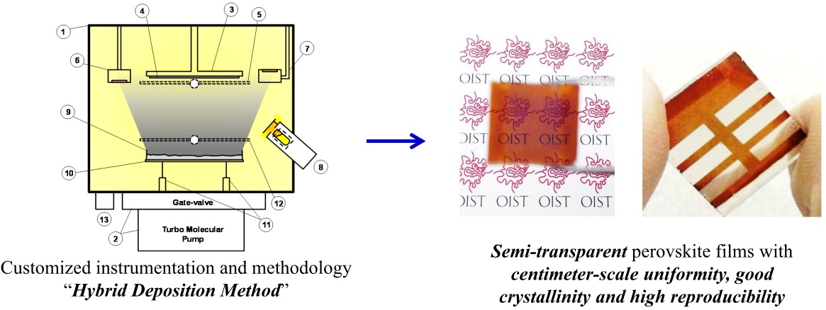
Figure 1: Schematic drawing showing the hybrid deposition instrumentation and picture of CH3NH3PbI3-xClx perovskite layer with semi-transparent property.
3.2 Fabrication of high-efficient and long-lasting perovskite films by the hybrid chemical vapor deposition method.
Matthew R. Leyden, Luis K. Ono, Sonia R. Raga, Yuichi Kato, Shenghao Wang and Yabing Qi *, "High Performance Perovskite Solar Cells by Hybrid Chemical Vapor Deposition", J. Mater. Chem. A 2, 18742-18745 (2014).
Yabing Qi, Matthew Leyden, US provisional patent application “System and method based on low-pressure chemical vapor deposition of perovskite films for solar cell applications” (2014).
Chemical vapor deposition is an inexpensive way to batch-process solar cells with good uniformity and facilitates low-cost production. Methylammonium lead iodide perovskite has small energy band gaps and greater potential efficiency for solar cell applications. In this work we introduce a new method of perovskite synthesis by hybrid chemical vapor deposition (HCVD), and demonstrate efficiencies as high as 11.8%. These cells were found to be stable with time, and retained almost the same efficiency after approximately 1100 h storage in dry N2 gas. This method is particularly attractive because of its semi-transparency and ability to scale up to industrial levels and the ability to precisely control gas flow rate, temperature, and pressure with high reproducibility. This is the first demonstration of a perovskite solar cell using chemical vapor deposition and there is likely still room for significant optimization in efficiency.
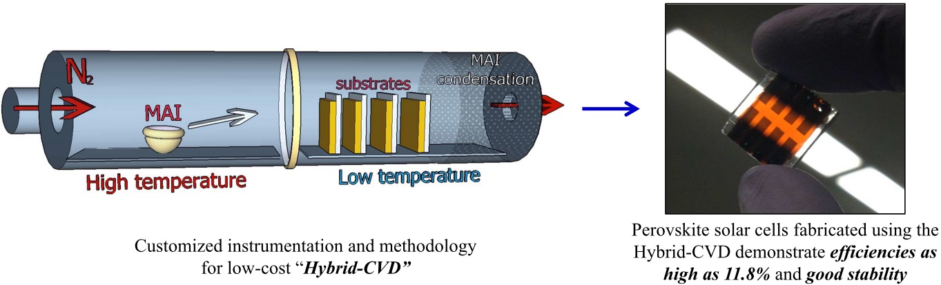
Figure 2: (Left) Schematic of a chemical vapor deposition system for the growth of perovskite on substrates pre-deposited with PbCl2. (b) Photograph of completed cell with a thin transparent gold top contact.
3.3 Influences of pinholes in spiro-MeOTAD hole transport layer on efficiency and stability of perovskite solar cells.
Zafer Hawash, Luis K. Ono, Sonia R. Raga, Michael V. Lee, and Yabing Qi *, "Air-Exposure Induced Dopant Re-distribution and Energy Level Shifts in Spin Coated Spiro-MeOTAD Films", Chem. Mater. 27, 562 (2015).
(OIST News, OIST Update - February 2015)
Min-Cherl Jung, Sonia R. Raga, Luis K. Ono and Yabing Qi*, "Substantial improvement of perovskite solar cells stability by pinhole-free hole tranport layer with doing engineering". Sci. Rep. 5, 9863 (2015).
(OIST News1, OIST News2, OIST Update - July 2015)
The stability of solar cells under storage and operation conditions is an important factor in determining the potential for commercial deployment as new photovoltaic technology. Despite all the superb properties of perovskite material, the reported data on the lifetime and degradation mechanisms of fabricated perovskite-based solar cells under operation conditions are limited, although degradation of the perovskite layer induced by ambient air/moisture, temperature and light exposure is evident. However, the degradation mechanism within the device is not well understood. Also, a perovskite solar cell contains several layers, all of which may play a role in the cell stability. For example, little attention has been given to the adjacent electron- and hole-transport layers (ETL and HTL) as well as top-electrode contacts (e.g. Ag, Al, etc.), which might fail faster than the active layer itself. Because in the majority of the perovskite solar cells, the HTL is the top-most layer (i.e. in direct contact with ambient air), the investigation of the physico-chemical property changes induced by air exposure on the HTL is important and need to be investigated systematically (humidity, temperature, and light intensity). 2,2’,7,7’-tetrakis(N,N-di-p-methoxyphenylamine)-9,9’-spirobifluorene (spiro-MeOTAD) is the most widely used HTL in current high performance solid-state cells, mostly due to its high stability (glass-transition temperature Tg = 121 °C), high solubility, and amorphous nature. We have found out that the HTL’s conductivity as well as interfacial energy levels are sensitively affected by the air exposure (O2 and/or H2O). In addition, these as-prepared spin coated films of spiro-MeOTAD showed a high density of pin-holes, which are detrimental for the underneath perovskite layer by facilitating the diffusion of H2O molecules inwards and attacking the perovskite layer.
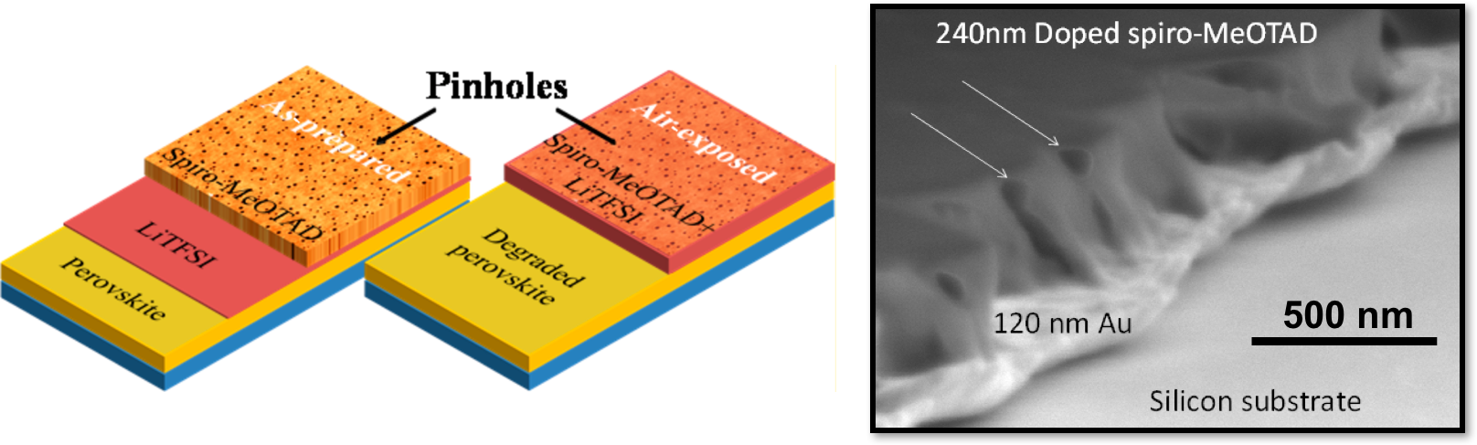
Figure 3: (Left) AFM images reveal the presence of pinholes with an average diameter of ∼135 nm and a density of ∼3.72 holes/μm2. (Right) Cross-sectional scanning electron microscope images reveal that these pinholes form channels across the doped spiro-MeOTAD film.
4. Publications
4.1 Journals
- M.C. Jung, S.R. Raga, L.K. Ono and Y. B. Qi*, "Substantial improvement of perovskite solar cells stability by pinhole-free hole transport layer with doping engineering". Sci. Rep. 5, 9863 (2015).
- S. R. Raga, M.-C. Jung, M. V. Lee, M. R. Leyden, Y. Kato, and Y. B. Qi*, "The influence of air annealing on high efficiency planar structure perovskite solar cells", Chem. Mater. 27, 1597 (2015).
- Z. Hawash, L. K. Ono, S. R. Raga, M. V. Lee, and Y. B. Qi*, "Air-Exposure Induced Dopant Re-distribution and Energy Level Shifts in Spin Coated Spiro-MeOTAD Films", Chem. Mater. 27, 562 (2015).
- L.K. Ono, S.R. Raga, S. Wang, Y. Kato, and Yabing Qi*, “Temperature-dependent hysteresis effects in perovskite-based solar cells”. J. Mater. Chem. A 3, 9074-9080 (2015).
- M.C. Jung, M.R. Leyden, G.O. Nikiforov, M.V. Lee, H.-K. Lee, T.J. Shin, K. Takimiya, and Yabing Qi*, “Flat-Lying Semiconductor–Insulator Interfacial Layer in DNTT Thin Films”. ACS Appl. Mater. Interf. 7, 1833-1840 (2015).
- G.O. Nikiforov, L.K. Ono, and Y.B. Qi*, "p-Doping of Squaraine with F4-TCNQ by Solution Processing", ITE Trans. on MTA 3, 133-142 (2015).
- H. Lee, Y.B. Qi, S. Kwon, M. Salmeron*, and J.Y. Park*, "Large changes of graphene conductance as a function of lattice orientation between stacked layers", Nanotechnology 26, 015702 (2015).
- M.C. Jung, D. Zhang, G.O. Nikiforov, M.V. Lee, T.J. Shin, D. Ahn, H.K. Lee, J. Baik, H.J. Shin, and Y.B. Qi *, "Ultrathin polycrystalline 6,13-Bis(triisopropylsilylethynyl)-pentacene films", J. Vac. Sci. Technol. A 33, 021506 (2015).
- M.R. Leyden, L.K. Ono, S.R. Raga, Y. Kato, S.H. Wang, and Y. B. Qi*, "High performance perovskite solar cells by hybrid chemical vapor deposition", J. Mater. Chem. A 2, 18742-18745 (2014).
- L.K. Ono, S. Wang, Y. Kato, S.R. Raga, and Y. B. Qi*, "Semi-Transparent Perovskite Films with Centimeter-scale Superior Uniformity by the Hybrid Deposition Method", Energy Environ. Sci. 7, 3989-3993 (2014).
- Moule, A.J., M.-C. Jung, C.W. Rochester, W. Tress, D. LaGrange, I.E. Jacobs, J. Li, S.A. Mauger, M.D. Rail, O. Lin, D.J. Bilsky, Y.B. Qi, P. Stroeve, L.A. Berben, and M. Riede, Mixed interlayers at the interface between PEDOT:PSS and conjugated polymers provide charge transport control. Journal of Materials Chemistry C 3, 2664-2676 (2015).
- Y.M. Lee, J. Baik, H.J. Shin, Y.S. Kim, S.G. Yoon, M.C. Jung, and Y.B. Qi, "Observation of chemical separation of In3Sb1Te2 thin film during phase transition", Appl. Surf. Sci. 292, 986-989 (2014).
- Y.M. Lee, D. Ahn, J.Y. Kim, Y.S. Kim, S. Cho, M. Ahn, M.H. Cho, M.S. Jung, D.K. Choi, M.C. Jung, and Y.B. Qi, "Only the chemical state of Indium changes in Mn-doped In3Sb1Te2 (Mn: 10 at.%) during multi-level resistance changes", Sci. Rep. 4, 4702 (2014).
- N.T. Ho, V. Senthilkumar, H.-S. Cho, S.H. Nho, S. Cho, M.C. Jung, Y.B. Qi, and Y.S. Kim, "Reliability improvement of bulk-heterojunction organic solar cell by using reduced graphene oxide as hole-transport layer", Phys. Stat. Solid A 211, 1873-1876 (2014).
4.2 Books and Other One-Time Publications
nothing to report
4.3 Oral and Poster Presentations
- Yabing Qi, “Perovskite film deposition by vapor-based methods for solar cell applications”, invited talk at the 2015 Materials Challenges in Alternative and Renewable Energy Conference (MCARE 2015), Jeju, Korea, February 24-27, 2015.
- Yabing Qi, “Perovskite Solar Cell Research Using a Surface Science Approach”, invited talk at National Institute for Materials Science, Tsukuba, Japan, February 17, 2015.
- Yabing Qi, “Uniform Perovskite Films by the Hybrid Deposition Method and Their Solar Cell Applications”, invited talk at University of Tokyo, Tokyo, Japan, August 6, 2014.
- Yabing Qi, “Semi-transparent perovskite films deposited by vapor-based methods and their solar cell applications”, invited talk at the 6th Asian Conference on Organic Electronics 2014 (A-COE 2014), Tainan, Taiwan, November 12-14, 2014.
5. Intellectual Property Rights and Other Specific Achievements
- Yabing Qi, Luis K. Ono, Shenghao Wang, US provisional patent application (2014).
- Yabing Qi, Luis K. Ono, Shenghao Wang, US provisional patent application (2014).
- Yabing Qi, Matthew Leyden, US provisional patent application (2014).
- Yabing Qi, Min-Cherl Jung, Sonia Ruiz-Raga, US provisional patent application (2014).
6. Meetings and Events
6.1 Seminar
- Date: July 12, 2014
- Venue: OIST Campus Lab1, C016
- Speaker: Dr. Pablo Boix, Energy Research Institute @ NTU (ERI@N, Singapore)
- Perovskite-based solar cells
- Date: July 24, 2014
- Venue: OIST Campus Lab1, C016
- Speaker: Prof. Iván Mora-Seró, Universitat Jaume I de Castelló, Spain
- Title: Dye and perovskite solar cells
- Date: July 24, 2014
- Venue: OIST Campus Lab1, C016
- Speaker: Prof. Francisco Fabregat-Santiago, Universitat Jaume I de Castelló, Spain
- Title: Dye and perovskite solar cells
- Date: September 21, 2014
- Venue: OIST Campus Lab1, C016
- Speaker: Dr. Saar Kirmayer, Department of Materials and Interfaces, Weizmann Institute of Science, Israel
- Title: High Open-Circuit Voltage Cells Based on Organic Lead Halide Perovskites
- Date: October 2, 2014
- Venue: OIST Campus Lab1, C016
- Speaker: Prof. Katsuhiko Ariga, World Premier International (WPI) Center for Materials Nanoarchitectonics (MANA), National Institute for Materials Science (NIMS), Tsukuba, Japan
- Title: Hand-Operating Nanotechnology: Can we control molecular machines by our hands?
- Date: November 10, 2014
- Venue: OIST Campus Lab1, C016
- Speaker: Prof. Thomas D. Anthopoulos, Department of Physics and Centre for Plastic Electronics, Blackett Laboratory, Imperial College London, London, UK
- Title: New Materials and Fabrication Paradigms for Plastic Opto/Electoronics
- Date: January 23, 2015
- Venue: OIST Campus Lab1, C016
- Speaker: Prof. Kilwon Cho, Chemical Engineering, Pohang University of Science and Technology (POSTECH), Republic of Korea
- Title: Surface-Directed Molecular Assembly of Organic Semiconductors for High-Performance Organic Electronics
- Date: January 23, 2015
- Venue: OIST Campus Lab1, C016
- Speaker: Prof. Tae-Woo Lee, Department of Materials and Engineering, Pohang University of Science and Technology (POSTECH), Republic of Korea
- Title: Organic/inorganic perovskite optoelectronics using self-organized polymeric buffer layers
- Date: January 24, 2015
- Venue: OIST Campus Lab1, C016
- Speaker: Dr. Shiyong Wang, EMPA, Swiss Federal Laboratories for Materials Science and Technology, Dübendorf, Switzerland
- Title: Atomic and electronic structure of bottom-up synthesized graphene nanoribbons characterized via non-contact atomic force microscopy and scanning tunneling microscopy.
- Date: January 27, 2015
- Venue: OIST Campus Lab1, C016
- Speaker: Prof. Furong Zhu, Department of Physics and Institute of Advanced Materials, Hong Kong Baptist University, Hong Kong
- Title: Enhanced Absorbance and Electron Collection in Inverted Organic Solar Cells.