

FY2012 Annual Report
Energy Materials and Surface Sciences Unit
Abstract
Energy materials will play a key role in the near future of the world's technology. The maturation of agriculture, manufacturing, and electronics have provided the essential needs and a continuously improving quality of life to an exploding population. However we still rely on combustion of fossil fuels for energy to drive the growth. Two keys to sustained growth are 1) to capture and effectively use the energy resources available to us, especially solar power, and 2) incorporation of less-expensive, processable, and customizable organics into electronics. Advancement of solar power requires reductions in cost that will likely come by introducing organic components, as well as understanding and optimization of the creation of excitons, dissociation into electrons and holes, and flow of charges especially at the interfaces. Integration of organics requires careful incorporation and analysis of their properties as electronic or photovoltaic components.
We apply surface science to provide sub-nanometer control over device fabrication as well as understanding of each of the interfaces and how they interact. Analysis of solar cells includes band structure and composition. Surface science for organic electronics includes controlling the crystallinity and molecular thickness of organic semiconductors, as well as analysis of chemical states. In collaboration with other groups at OIST we apply surface science to image the structure and analyze the surface properties of biological surfaces.
1. Staff
- Dr. Michael Lee, Group Leader
- Dr. Min-Cherl Jung, Researcher
- Dr. Haijun Fan, Researcher
- Cristina Chiutu, Researcher
- Alison Cross, Graduate Student (Exchange program)
- Jiu Xu, Undergraduate Student (Exchange program)
- Dongrong Zhang, OIST Graduate Student
- Taki Tazuke, Secretary
2. Collaborations
- Theme: Phosphorescent OLEDs with Low Operating Voltage
- Type of collaboration: Cowork
- Collaborators:
- Ming Liu & Shi-Jian Su, South China University of Technology
- Wei-Ming Zhao, Dongguan LITEWELL Technology Incorporation
- Junji Kido, Yamagata University
- Theme: Study on atomic and electronic structures of organic-based thin layers studied with synchrotron radiation
- Type of collaboration: Cowork (ongoing)
- Collaborators:
- Beamline manager, Dr. Young Mi Lee, Pohang Accelerator Laboratory
- Beamline manager, Dr. Han-Koo Lee, Pohang Accelerator Laboratory
- Beamline manager, Dr. Hyun-Joon Shin, Pohang Accelerator Laboratory
- Theme: Investigation of surface morphology and mechanical property of cancer cells by AFM
- Type of collaboration: Cowork (ongoing)
- Collaborators:
- Prof. Tadashi Yamamoto, Cell Signal Unit/OIST
- Dr. Yo-taro Shirai, Cell Signal Unit/OIST
3. Activities and Findings
3.1 Organic Light Emitting Diode (OLED)
Characterization of new materials for low operating voltage OLED devices [Dr. Jung]
Organic light-emitting devices (OLEDs) have become of considerable commercialization interest in recent years for their applications as eco-friendly solid-state lighting and next generation full-color flat-panel displays. In the last two decades, many studies have focused on improving external quantum efficiency (ηext) of OLEDs, and phosphorescent OLEDs have attracted tremendous attention since nearly 100% internal quantum efficiency of electroluminescence is readily achieved by harvesting both electro-generated singlet and triplet excitons. It is well-known that at a given ηext lower operating voltage generally gives higher power conversion efficiency. As such, lowering operating voltage is also crucially important to reduce their electrical power consumption. It has been reported that OLEDs with p-doped hole-transport layer (HTL) and n-doped electron-transport layer (ETL), called p-i-n OLEDs, generally exhibit low driving voltage as well as high power efficiency. However, carrier and exciton block layers are absolutely essential to prevent exciton quenching in the emissive layer (EML) by the p and n dopants, and the internal energy barriers to overcome the carrier and exciton block layers may induce voltage drop and thus higher operating voltage. More importantly, the approach of using n dopant-like alkaline metals might be hampered by stability issues and leads to manufacturing difficulties. It is thus of interest to utilize a single carrier transport layer instead of p- or n-doped layer and carrier/exciton block layer. In the past years, a series of multifunctional pyridine-containing electron-transport materials (ETMs) have been developed as an ETL as well as a hole/exciton block layer for the phosphorescent OLEDs, leading to a simplified device structure and an improved ηext. Most recently, operating voltages that are readily lower than those of the p-i-n OLEDs were also achieved by utilizing 1,3,5-triazine-containing ETMs. A general character for all these ETMs is that they have pyridine rings on the periphery of the molecule and the substituted positions of the pyridine rings in a single molecule are identical. Since the nitrogen atom position of the substituted pyridine ring was found to be a key factor in determining the electron injection and transport property and thus the OLED performance, it is of interest to synthesize pyridine-containing compounds with different pyridine substitution positions in a single molecule to further tune the property of the pyridine-containing ETMs. Besides this, simultaneous introduction of other heterocycles to give hybrid heterocycle-containing compounds is also an attractive approach to tune their property.
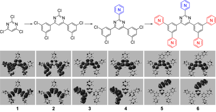
Figure 1: Synthetic Routes of Pyridine-Containing Compounds and calculated frontier orbitals of the HOMO (bottom) and LUMO (top)
A series of hybrid heterocyle-containing ETMs with different pyridine substitution positions in a single molecule were successfully synthesized by regioselective sequential palladium-catalyzed Suzuki crosscoupling reactions. B3LYP calculations show that the experimental regioselectivity is consistent with the trends in calculated bond dissociation energies of the carbon−halogen (C−X) bonds of the reactants and intermediates. The two carbon species associated with C−N and C−C can be detected by X-ray photoelectron spectroscopy. Extremely low turn-on voltages (Von) of 2.1 V for electroluminescence, which are readily 0.2−0.3 V lower than the minimum value of the emitted photon energy (hv)/e, were experimentally achieved by utilizing the developed ETMs as an electron-transport and hole/exciton-block layer for the classical fac-tris(2-phenylpyridine) iridium (Ir(PPy)3)-based green phosphorescent organic light-emitting devices (OLEDs). In addition, hitherto the lowest operating voltages of 2.39, 2.72, and 3.88 V for 100, 1000, and 10 000 cd m−2 were achieved with simultaneously improved external quantum efficiency (ηext) to give a high power efficiency, and the operating voltage for 100 cd m−2 is already corresponding to the value of hv/e. Atomic force microscopy measurements reveal morphological fine structure of the thin film samples of ETMs with a pyrimidine core, which possibly contributes to the low driving voltages that were achieved for the devices that are based on these ETMs. These findings indicate that aside from the ultralow operating voltage wellbalanced carriers can be also achieved with a finely synthesized hybrid heterocyle-containing ETM as a nondoped electrontransport layer and the B3LYP calculation is an effective method to predict the regioselective cross-coupling reactions for fine design of such an ETM.
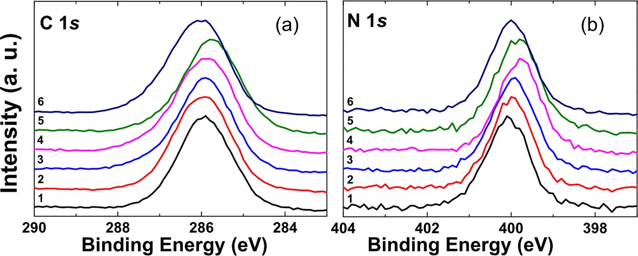
Figure 2: (a) C 1s and (b) N 1s core-level spectra of ETMs 1-6.
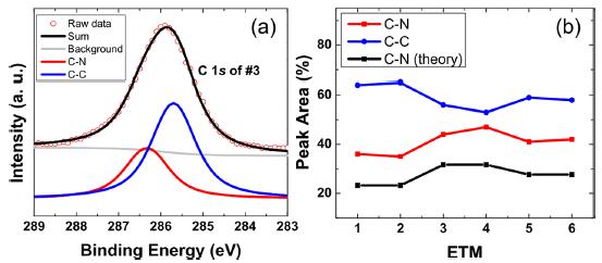
Figure 3: (a) Curve fitting for C 1s of thin film sample of ETM 3. (b) Peak area of the two C species (C-N and C-C) for the thin film samples of ETMs 1-6.
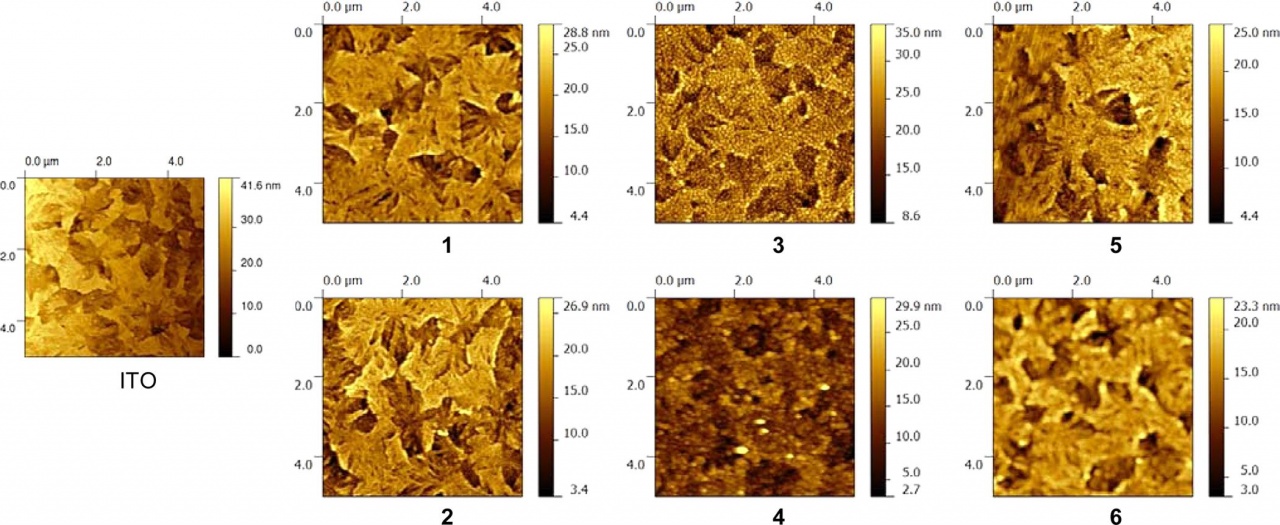
Figure 4: AFM images of the bare ITO substrate and the thin film of 1-6 vacuum deposited on ITO.
3.2 Organic-based thin-film transistor (OTFT)
Optimization of ultra-thin TIPS-Pentacene films [Mr. Zhang and Dr. Jung]
As now well known, the carrier mobility of organic films plays a significant role in OTFTS efficiency. Recently, 6,13-bis(triisopropylsilylethynyl)(TIPS)-Pentacene has attracted much interest due to its high mobility (1.8 ~ 5 cm2/V·s) and stability in air. In addition, deposition of TIPS-Pentacene can be realized by an easier method like spin-coating and inkjet-printing in virtue of its solubility. This work focused on the controlling of deposition conditions to obtain ultra-thin and high-coverage TIPS-Pentacene films supposed to show better mobility for devices fabrication. We also compared spin-coating results in nitrogen to air.
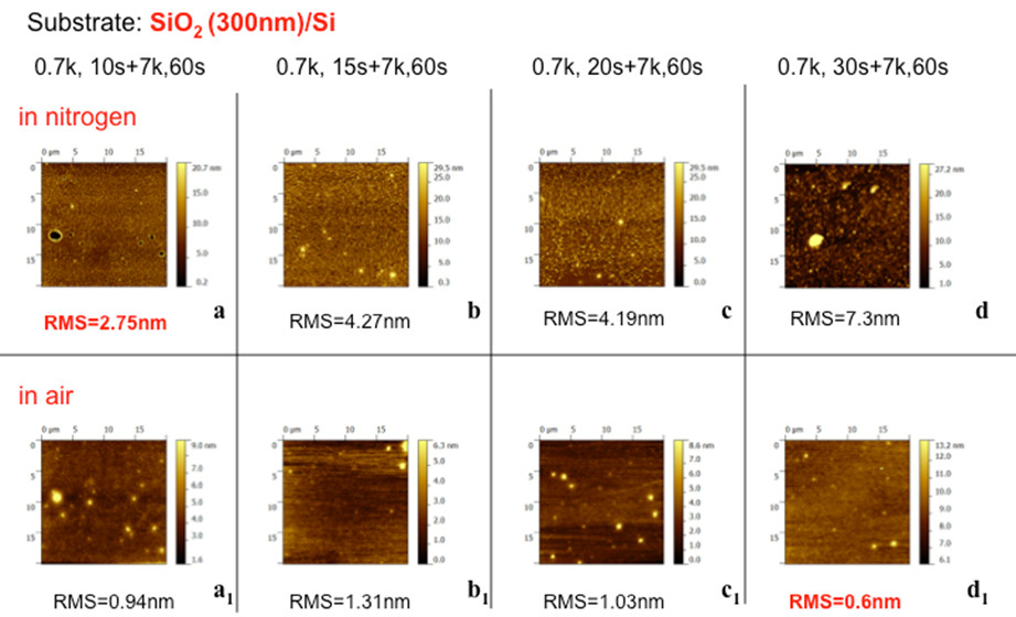
Figure 5: Surface morphology comparison of TIPS-Pentacene thin film deposited in nitrogen and in air under various deposition conditions
Figure 5 shows that two-step spin-coating results in nitrogen and air are quite different. In general, the roughness in air is better and the films in air are thinner than those deposited in nitrogen. With the fixed second step, 7k rpm for 60s, we varied the first step condition, 0.7k rpm for 10s, 15s, 20s and 30s, to find the best result.
Figure 6 shows detailed information of d1 and a, which have the smallest roughness. d1' and a' are zoomed in from d1 and a respectively. This ultra-thin film d1' is only around 1.5 nm, much thinner compared to that 7 nm film a. Both d1' and a' have a high coverage more than 80%.
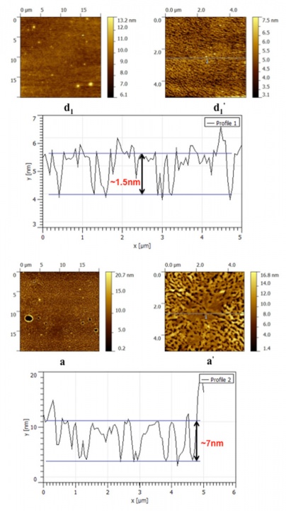
Figure 6: Detailed surface morphology and profiles of a and d1 in Figure 1
3.3 Organic-based Solar Cells (OSC)
Thermal Annealing of OSCs [Jiu Xu, Alison Cross, Dr. Lee]
This research interest mainly involves optimization of photovoltaic device performance, and further understanding of the physical processes involved in organic photovoltaics, especially those processes occurring at the surface and interfaces. Herbert Kroemer, a Nobel laureate, summarized the observations of many researchers on electronic processes with the famous phrase “the interface is the device”. Realizing its importance, we also focus on the interfaces in solar devices.
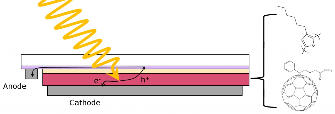
Figure 7: The structure of typical P3HT:PCBM solar cell.
The polymeric/small molecule components of solar cells (see Figure 7) were investigated for morphological change under differing annealing conditions. Thin films of PEDOT:PSS, P3HT and a blend of P3HT with PCBM were deposited on to ITO substrate by spin coating. The films were annealed at either a slow or fast rate of heating to a set target temperature and then with cooled slowly or quickly. Each of the possible permutations were investigated with identical films. Figure 8 shows that when rapidly cooled (regardless of heating rate) unusual morphologies were observed in films of PEDOT:PSS and when PEDOT:PSS was present under a different thin film layer. The morphologies of the films were analysed by both optical microscopy and atomic force microscopy. Annealing not only produces changes in the structure of the film layers, but also changes the efficiency of devices. We have not yet found direct correlation between structure changes and efficiency.
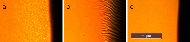
Figure 8: a) A non-annealed device after vacuum aluminum evaporation. b) A device with fast cooling after fast heating to 110 oC. c) A device with slow cooling after fast heating to 110 oC.
Lifetime of OSCs [Dr. Fan, Dr. Lee]
The short lifetime of organic solar cell devices is a significant obstacle preventing commercialization. We have observed this effect in solar cells in our laboratory. Even over just a three days, a drop of around 30% can be observed even for cells that are stored in a glove box. Alternatively, if films are spin-coated from solutions that have been stored in the glove box for an extended period of time, the films show almost complete oxidation. This is observed by X-ray Photoelectron Spectroscopy of the sulfur peak from P3HT:PCBM films. These oxidation effects are shown in Figure 10. The inert environment of the glove box should provide significant protection against attack by oxygen or water. These experiments suggest that the oxidation may come from an interaction between the donor and acceptor themselves. More stable donor and acceptor molecules or possibly an intermediate between donor and acceptor may be able to extend the lifetime of organic devices.
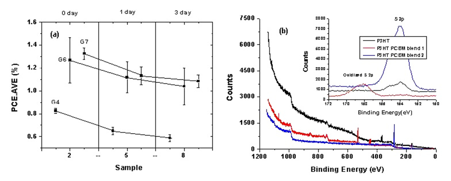
Figure 9. (a) Decrease in device performance over time. (b) XPS of films from fresh P3HT solution, fresh P3HT:PCBM solution (blend 2), and 25-day-old P3HT:PCBM solution stored in the glove box (blend 1).
We have come to several conclustions:
- The heating and cooling rates affect the structure of a PEDOT:PSS film.
- The heating and cooling rates during annealing affect the efficiency of energy conversion in organic solar cells.
- Oxidation of P3HT or other donor molecules could play an important role in the degradation of organic solar cells.
3.4 Interdisciplinary collaborations
Mechanical Analysis of Cancer Cells by Atomic Force Microscope [Ms. Chiutu]
The process involved in tumor invasion and metastasis has been under continuous investigation and research studies. Numerous experiments have been conducted to understand the morphology and migration mechanism of cancer cells.
Atomic Force Microscopy plays an important role in determining the elastic and topographic properties of cancer and normal cells. Biomechanics of cancer cells has proven to be strongly related to cell structural and functional properties. Being able to distinguish between cells just by knowing the stiffness would be a great advance in cancer diagnosis. Morphology of various cells may provide useful information about structure evolution and physiological process of a cell. Atomic Force Microscopy produces high resolution images of cell membrane.
Recently, in our group, we started a collaboration project on biophysics experiments with Cell Signal Unit. The purpose of this research work is to compare the mechanical properties between human pancreatic cancer cells and pancreatic epithelial healthy cells. For this reason, we use Atomic Force Microscope to achieve detailed resolution of the cell topography and structure. Furthermore, we probe the cell stiffness by force spectroscopy using silicon, gold and functionalized tips. All experiments are performed in air at this stage. A future goal is to scan and measure force spectra on living cells.
4. Publications
4.1 Journals
M. Liu, S.-J. Su*, M.-C. Jung, Yabing Qi*, W.-M. Zhao, and J. Kido, Chemistry of Materials 24, 3817–3827 (2012).
4.2 Books, book chapters and other one-time publications
Yabing Qi, “Doping in organic semiconductors”, invited Section Editor and book chapter in Encyclopedia of Nanotechnology, Springer-Verlag (2012).
4.3 Oral and Poster Presentations
-
Yabing Qi, “Organic films and their applications in organic electronics”, Invited talk at Soochow University, China, July 2, 2012.
-
Yabing Qi, “Spectroscopic and charge transport investigations on organic films”, Invited talk at Sichuan University, China, July 9, 2012.
-
Yabing Qi, “Energetics and charge transport in organic films”, Invited talk at Xi'an Jiaotong University, China, July 16, 2012.
-
Yabing Qi, “Investigating Organic Electronics with a Surface Science Approach”, Invited talk at Yangzhou University, China, August 2, 2012.
-
Yabing Qi et al., “Highly crystalline ultrathin films of TIPS pentacene”, Invited talk at 9th International Conference on Electroluminescence & Organic Optoelectronics, Fukuoka, September 6, 2012.
-
Yabing Qi, “Temperature Dependent Growth of Organic Thin Films”, Invited talk at 1st International Symposium of the Advanced Graduate Program on Molecular Systems for Devices, Fukuoka, March 29, 2013.
-
Min-Cherl Jung and Yabing Qi, “Introduction of organic thin-film transistor studied in Okinawa Institute of Science and Technology Graduate University”, CAS-PSOC Beijing Summer Workshop 1st, Beijing, China (June 12. 2012). (Invited oral presentation).
-
Min-Cherl Jung and Yabing Qi, “Fabrication and characterization of ultra-thin TIPS-Pentacene film by spin-casting”, International Symposium of organic Electronics 2012, Okinawa, Japan (October 4. 2012). (Poster presentation).
5. Intellectual Property Rights and Other Specific Achievements
Yabing Qi has been invited to join the Editorial Board of Scientific Reports, which is a research publication from the Nature Publishing Group covering all areas of the natural sciences.
6. Meetings and Events
6.1 International Symposium on Organic Electronics 2012 (ISOE2012)
Energy Materials and Surface Sciences Unit and OIST's Workshop Section hosted the first International Symposium on Organic Electronics (ISOE 2012) from October 3-5, 2012. We brought scientists from physics research, chemistry research, and industry together in order to discuss key questions relating to organic electronics. The fifteen invited speakers represent the breadth and diversity of this key technological discipline at the highest international standard. Thirty early career scientists also attended the symposium as poster participants to learn from the leaders in the field and brought their enthusiasm for discovery. ISOE 2012 was held at OIST's Seaside House and included excursions to OIST main campus and also to Okinawa's Churaumi Aquarium to provide a beautiful and relaxing subtropical setting to encourage free-form interaction.
Invited Speakers
- J. Takeya, Osaka University, Japan
- K. Takimiya, Hiroshima University, Japan
- A. Facchetti, Northwestern University, USA
- C. Adachi, Kyushu University, Japan
- A. Kahn, Princeton University, USA
- S. R. Marder, Georgia Institute of Technology, USA
- T. D. Anthopoulos, Imperial College London, UK
- N. Ueno, Chiba University, Japan
- N. Koch, Humboldt University of Berlin, Germany
- C. Luscombe, University of Washington, USA
- C. I. Wu, National University of Taiwan, Taiwan
- D. Cahen, Weizmann Institute of Science, Israel
- T. Kato, University of Tokyo, Japan
- H. Murata, Japan Advanced Institute of Science and Technology, Japan
- Y. Ie, Osaka University, Japan
Chair
Prof. Yabing Qi, OIST, Japan
Co-organisers
Prof. Yoshio Aso, Osaka University, Japan
Prof. Jun Takeya, Osaka University, Japan
Prof. Kazuo Takimiya, Hiroshima University, Japan
Prof. Antonio Facchetti, Northwestern University and Polyera Corporation, USA
Prof. Chihaya Adachi, Kyushu University, Japan
6.2 Seminar
- Date: April 16, 2012
- Venue: OIST Campus Lab1
- Speaker: Christina Chiutu (Nanoscience Group, School of Physics and Astronomy, University of Nottingham, United Kingdom).
- Date: April 20, 2012
- Venue: OIST Campus Lab1
- Speaker: Adam Sweetman (School of Physics, University of Nottingham, Kings College London Strand, London).
- Date: May 21, 2012
- Venue: OIST Campus Lab1
- Speaker: Yuichi Kato (Graduate School of Engineering, Kyushu University, Fukuoka, Japan).
- Date: June 15, 2012
- Venue: OIST Campus Lab1
- Speaker: Prof. Liang-Yao Chen (Department of Optical Science and Engineering, Fudan University, China).
- Date: August 16, 2012
- Venue: OIST Campus Lab1
- Dr. Liyu Liu (Institute of Physics, Chinese Academy of Sciences and Department of Physics, Princeton University).
- Date: September 21, 2012
- Venue: OIST Campus Lab1
- Dr. Aitor Mugarza (Catalan Institute of Nanoscience and Nanotechnology (ICN2), Barcelona, Spain)
- Date: January 25, 2013
- Venue: OIST Campus Lab1
- Prof. Naotoshi Nakashima (Department of Applied Chemistry & WPI-I2CNER & JST-CREST, Kyushu University)