Diamond Superconductivity and its Josephson Junction and SQUID

Date
Description
Quantum Machines Unit - Zoom Seminar open to OIST
Diamond Superconductivity and its Josephson-Junction and SQUID
Abstract: Diamond Superconductivity and its Josephson Junction and SQUID Superconducting quantum interference device (SQUID) is a magnetic sensor capable of detecting extremely small magnetic field and has already been used in various fields such as material science, medical equipment, mineral exploration, and so on. In addition, SQUID has also been used in qubit. Especially in Xmon qubit [1] which is a kind of transmon qubit [2] used for quantum computer, SQUID is an important component enabling to tune qubit frequency. General problems with SQUID's materials are temperature change, natural oxidation, and deterioration due to collision. Hence, we have fabricated a highly robust SQUID with heavily boron doped (8x1021 cm-3) diamond [3,4] which exhibits type II superconducting with Tc offset>10K has demonstrated SQUID operation [5,6]. Furthermore, boron-doped diamond enables SQUID operation under high magnetic field because of its high upper critical field which is estimated to be H2(0) = 11.5 T [7]. Among such demonstrations, the SQUID composed of the trench-type or step-type Josephson junctions (JJs), which were formed in the boundary of discontinuous (111) sectors, operated at 10 K above liquid helium temperature (4.2 K) [6]. Unlike the previous structure included (001) surface (Tc < 4.2 K) [5], these trench or step-type JJs were composed of only (111) surface (Tc = 10K) [3,7]. At present Vp-p=47.7 μV at 1.6 K is the highest value in diamond SQUIDs. One of the unique properties of diamond is the close coexistence of superconductivity and two-dimensional Hall gas (2DHG) [8]. 2DHG diamond field effect transistors (FETs) exhibit high power microwave operation [9]. All diamond Josephson (Jo) FET that exhibits gate control on the Josephson coupling ultimately leads to the realization of electrically tunable transmon qubits [10] (gatemon).
[1] R. Barends, C. Neill et al., Phys. Rev. Lett. 111 (2013) 080502.
[2] J. Koch, R.J. Schoelkopf et al., Phys. Rev A 76 (2007) 042319.
[3] A. Kawano HK et al. Phys. Rev. B,82 (2010) 085318
[4] M.Watanabe, HK, Phys. Rev. B,85 (2012) 184516
[5] T. Kageura, HK et al., Sci. Rep. 9, (2019) 15214
[6] A. Morishita, HK et al., International Conference on Solid State Devices and Materials Abstract, PS-9-02 (2019) (submitted to a journal)
[7] T. Kageura, HK et al., Diamond and Related Materials 90 (2018) 181.
[8] S. Imanishi HK et al. IEEE Elec. Dev. Lett. 42 (2021) (in press).
[9] S. Imanishi HK et al. IEEE Elec. Dev. Lett. 40 (2019) 279. [10] T..Larsen, C. M. Marcus et al. Phys. Rev. Lett. 115 (2015) 127001. .
Biography
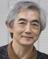
Hiroshi Kawarada is Professor of Department of Electronics & physical Systems and Department of Nanoscience & Nanotechnology at Waseda University. He received B.S., M.E. and Doctor of Engineering (1985) at Waseda University. Between 1986-1990, he was Assistant Professor in Osaka University. From 1990, he joined Waseda University as Professor.
Registration
Attendees must register here to attend the zoom meeting. Note this meeting will not be recorded. This seminar is hosted by Prof Jason Twamley.
Subscribe to the OIST Calendar: Right-click to download, then open in your calendar application.


