

Photoemission Electron Microscopy
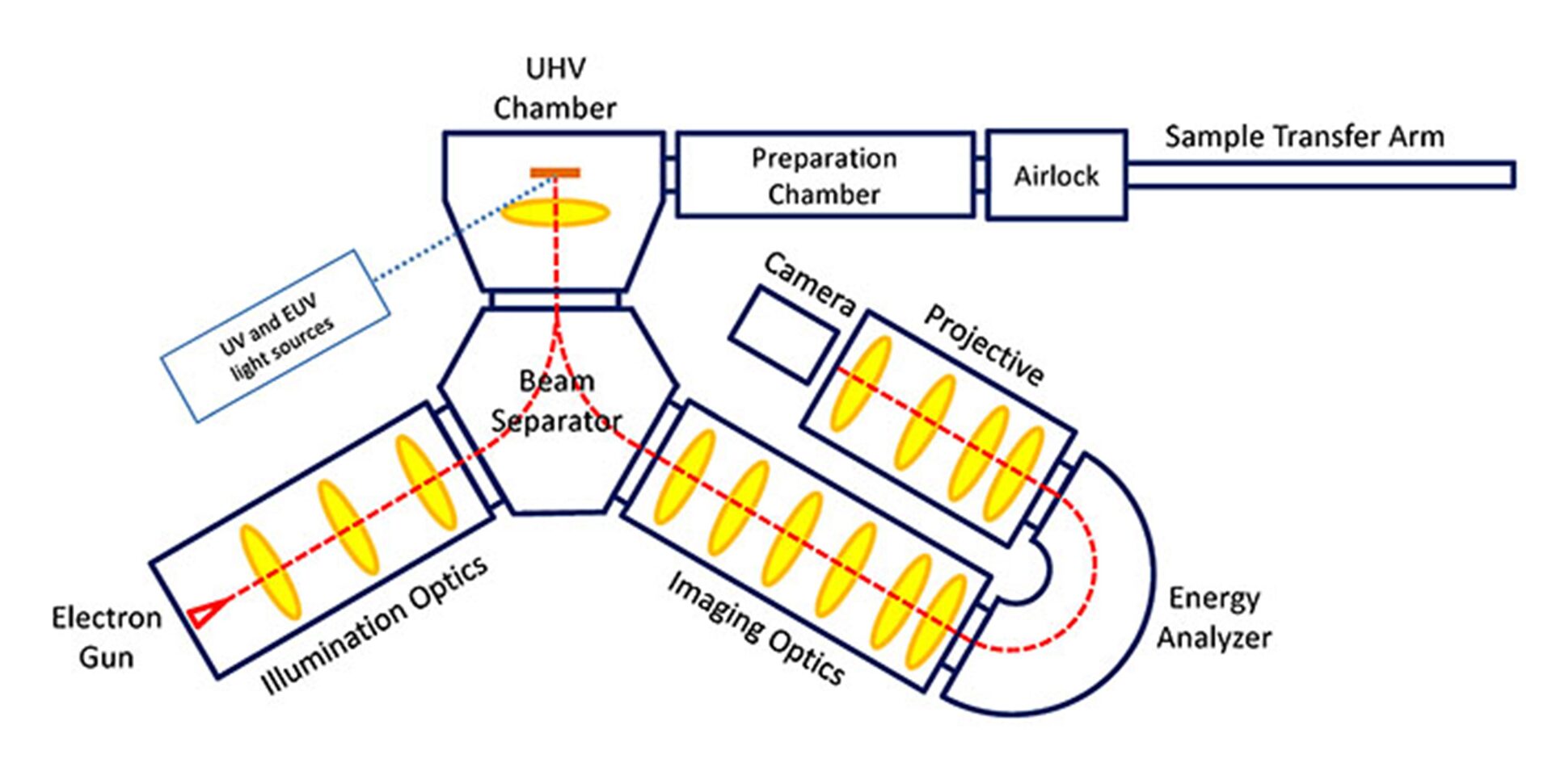
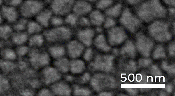
The aberration corrected SPELEEM we have installed in the microscopy lab is a unique electron microscope, it is capable of extracting structural, electronics, chemical and elemental information at spatial resolution down to a few tens of nanometers. Equipped with a LaB6 electron cathode, we can image elastically backscattered low energy electrons reflected from surfaces via low energy electron microscopy (LEEM) technique. Due to large backscattering cross sections of low energy electrons and non-scanning imaging principle of the cathode immersion lens design, we can image in real-time at video frame rate. It is an ideal instrument for monitoring in situ dynamic processes, such as growth and self-organization of nanostructures and thin films. With the aberration correction optics, lateral resolution of our LEEM is better than 2nm.
Contrast mechanisms in LEEM
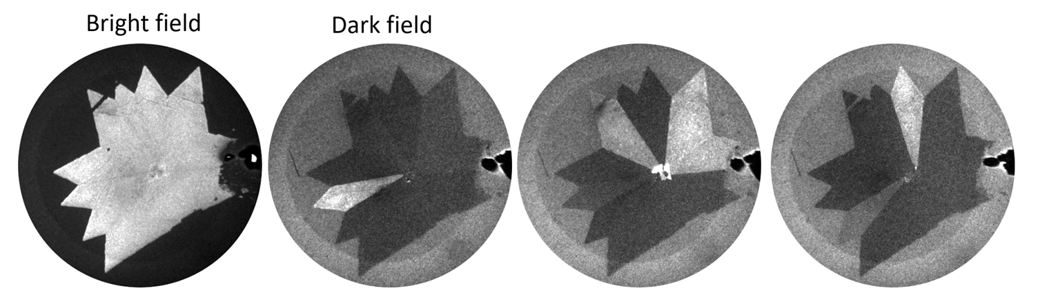
In LEEM, images are formed due to different diffraction and phase contrast mechanisms. We can do bright field imaging using the spectral diffracted beam, here local variation of the sample structure will provide diffraction contrast. We can also image with the non-specular diffracted beams, the so-called dark field imaging technique is very useful for the identification of coexisting crystal phases of different rotational variants.
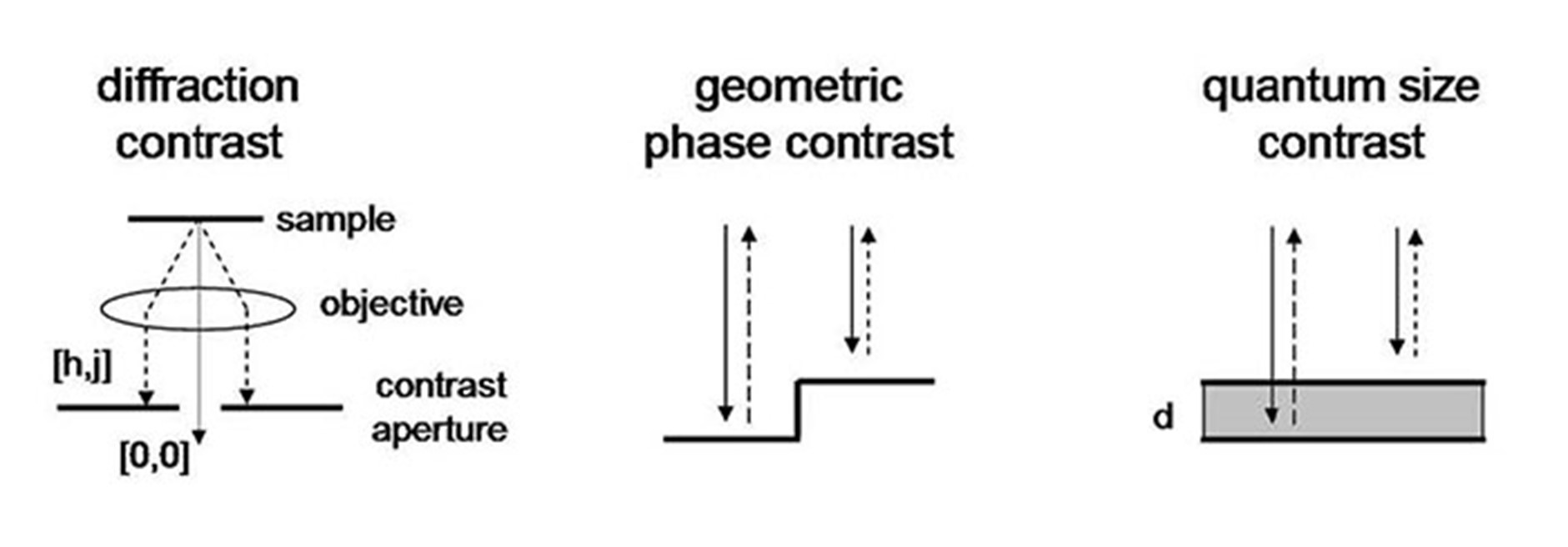
Changes in surface topology or potential variation could induce a local phase shift in the reflected electrons and cause the so-called phase contrast. For example, the height difference of atomic steps on surface will introduce a phase difference in the backscattered electron waves, interference of these waves provide contrast and allows us to image atomic steps. Another example we often see is the contrast in thin films or 2D layered materials of varying thickness, here the contrast is coming from interference between electron waves which are backscattered from the surface and the thin film/substrate interface. Depending on thin film thickness and the electron energy, we can observe maxima and minima in the scattered electron intensity. This mechanism allows quantitative measurement of film thickness on surfaces.
Low energy electron diffraction (LEED)
Besides direct imaging of surfaces, we can also image in reciprocal space and it gives access to low energy electron diffraction (LEED). LEED is one of the most important techniques for studies of crystalline structure in material surfaces. In our electron microscope, we can limit the footprint of the electron beam to <250nm by inserting a small aperture in the beam path of the electron cathode. This allows us to do micro-LEED (µ-LEED). We applied this technique in the investigation of structural deformation [1] and phase transition [2] in atomically thin 2D materials.
[1] M. K. L. Man, et al., Scientific Reports 6, 20890 (2016).
[2] M. Rumo et al., Phys. Rev. B 101, 235120 (2020).
Photoemission electron microscopy (PEEM)
Besides imaging using the electron cathode, in the same electron microscope, we can also image sample surfaces using photoelectrons generated by UV or x-ray light sources through the photoelectric effect. Photo-emitted electrons carry information about the chemical and electronic environment from where they are emitted from. Photoemission technique provides information such as valence energy levels and chemical bonding state of the near surface region of the sample. With the imaging energy analyzer, we can perform spatially resolved photoemission spectroscopy (PES/UPS/XPS) at lateral resolution better than 15nm and at energy resolution better than 150meV. In the last few years, we have applied our PEEM technique in the study of hybrid halide perovskite photovoltaic, to identify different kinds of defect clusters and to understand their relationship to charge trapping and performance losses [1-3]
[1] S. Macpherson et al., Nature 607, 294-300 (2022).
[2] S. Kosar et al., Enery Environ. Sci. 14, 6320-6328 (2021).
[3] T.A.S. Doherty et al., Nature 580, 360 (2020).
Besides looking at sample surfaces in real space, in the same microscope we can also image in the reciprocal space to resolve the photo electrons emitted at different azimuthal and polar angles and at different energy. This allows us to do photo-emitted electron diffraction/angle-resolved photoemission spectroscopy (PED/ARPES), and study electronic structures and reconstruct the entire 3D Fermi surfaces with high spatial resolution.
In our laboratory, several UV light sources are currently available. Surface imaging can be done with a quasi-CW UV laser or an ultrafast pulsed UV laser, while ARPES can be done using a He plasma discharge light source or an ultrafast pulsed extreme UV HHG light source.