

Opto-electronic phenomena in van der Waals heterostructures
In 2004, Novoselov and Geim successfully isolated the new the wonder material graphene, a single atomic layer of graphite, leading to the 2010 Nobel Prize. Graphene, with its remarkable properties [1,2] – a zero-bandgap semiconductor, record-high thermal and electrical conductivities, and relativistic dispersion for its electrons, launched the field of two-dimensional van der Waals (vdW) materials. Soon, other novel vdW materials were discovered with complementary properties, such as the semiconducting transition metal dichalcogenides (TMDs) [3] and the insulating hexagonal boron nitride (hBN). With the rapidly growing range of vdW materials, an intriguing idea was proposed by Geim and Grigorieva [4] – what if we can re-stack layers of different vdW materials together to combine complimentary properties into one heterostructure, or to create new physics at the interface of the disparate materials?
Over the past 5 years, the Femtosecond Spectroscopy Unit has explored a range of different vdW heterostructures and their properties, such as the ultrafast transient response of hBN/graphene heterostructures to observe dissipationless, photocapacitive behavior, second harmonic generation from multi-layer InSe, using atomically-thin hBN to decouple the interactions between MoS2 and the SiO2 substrate, and incorporating monolayer MoS2 into organic light harvesting devices to obtain enhanced photogenerated carrier generation.
Finally, to push the boundaries of our understanding of interface physics, since the inception of our unit 5 years ago, we embarked on a technically challenging project to combine ultrafast optics with photoemission electron microscopy techniques to successfully image the dynamics of carriers across semiconductor interfaces with simultaneous femtosecond-scale temporal and nanometer-scale spatial resolution.
Below we list some of our recent publications exploring opto-electronic phenomena in vdW heterostructures.
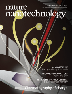
Imaging the Motion of Electrons Across Semiconductor HeterojunctionsNat. Nanotechnol. 12, 36 (2017). Technological progress since the late twentieth century has centred on semiconductor devices, such as transistors, diodes and solar cells. At the heart of these devices is the internal motion of electrons through semiconductor materials due to applied electric fields or by the excitation of photocarriers. Imaging the motion of these electrons would provide unprecedented insight into this important phenomenon, but requires high spatial and temporal resolution. Current studies of electron dynamics in semiconductors are generally limited by the spatial resolution of optical probes, or by the temporal resolution of electronic probes. Here, by combining femtosecond pump–probe techniques with spectroscopic photoemission electron microscopy, we imaged the motion of photoexcited electrons from high-energy to low-energy states in a type-II 2D InSe/GaAs heterostructure. At the instant of photoexcitation, energy-resolved photoelectron images revealed a highly non equilibrium distribution of photocarriers in space and energy. Thereafter, in response to the out-of equilibrium photocarriers, we observed the spatial redistribution of charges, thus forming internal electric fields, bending the semiconductor bands, and finally impeding further charge transfer. By assembling images taken at different timedelays, we produced a movie lasting a few trillionths of a second of the electron-transfer process in the photoexcited type-II heterostructure—a fundamental phenomenon in semiconductor devices such as solar cells. Quantitative analysis and theoretical modelling of spatial variations in the movie provide insight into future solar cells, 2D materials and other semiconductor devices
|
|
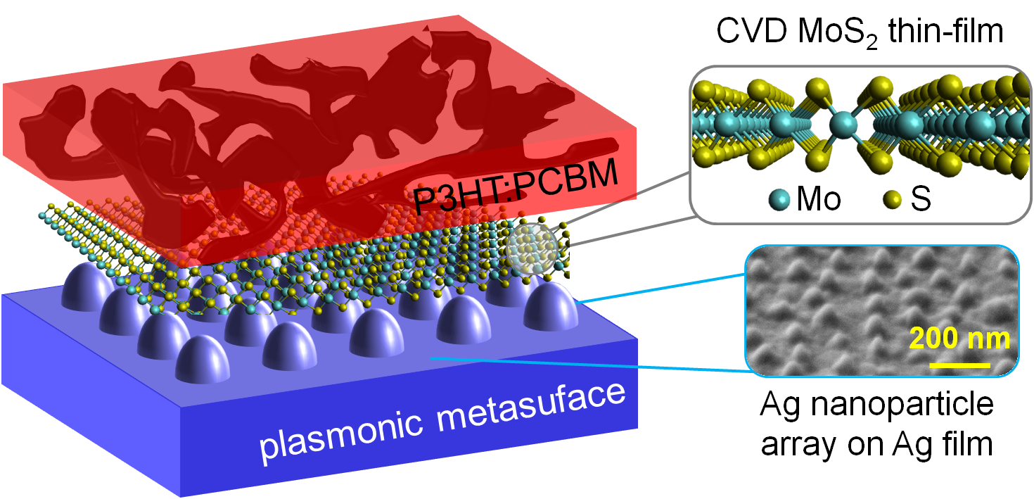
Ultrafast Charge Transfer and Enhanced Absorption in MoS2 - Organic van der Waals Heterojunctions Using Plasmonic MetasurfacesHybrid organic−inorganic heterostructures are attracting tremendous attention for optoelectronic applications due to their low-cost processing and high performance in devices. In particular, van der Waals p−n heterojunctions formed between inorganic two-dimensional (2D) materials and organic semiconductors are of interest due to the quantum confinement effects of 2D materials and the synthetic control of the physical properties of organic semiconductors, enabling a high degree of tunable optoelectronic properties for the heterostructure. However, for photovoltaic applications, hybrid 2D−organic heterojunctions have demonstrated low power conversion efficiencies due to the limited absorption from constraints on the physical thickness of each layer. Here, we investigate the ultrafast charge transfer dynamics between an organic polymer:fullerene blend and 2D n-type MoS2 using transient pump−probe reflectometry. We employ plasmonic metasurfaces to enhance the absorption and charge photogeneration within the physically thin hybrid MoS2−organic heterojunction. For the hybrid MoS2−organic heterojunction in the presence of the plasmonic metasurface, the charge generation within the polymer is enhanced 6-fold, and the total active layer absorption bandwidth is increased by 90 nm relative to the polymer:fullerene blend alone. We demonstrate that MoS2−organic heterojunctions can serve as hybrid solar cells, and their efficiencies can be improved using plasmonic metasurfaces.
|
|
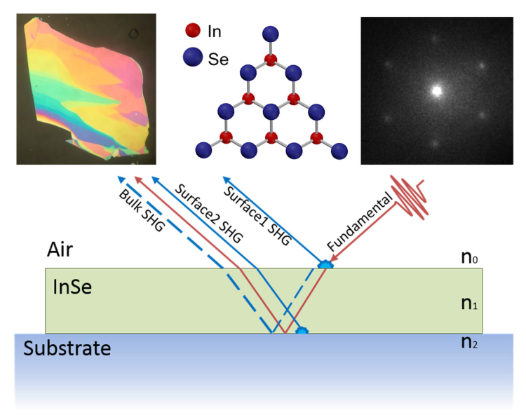
Observing the Interplay Between Surface and Bulk Optical Nonlinearities in Thin Van der Waals CrystalsVan der Waals materials, existing in a range of thicknesses from monolayer to bulk, allow for interplay between surface and bulk nonlinearities, which otherwise dominate only at atomically-thin or bulk extremes, respectively. Here, we observe an unexpected peak in intensity of the generated second harmonic signal versus the thickness of Indium Selenide crystals, in contrast to the quadratic increase expected from thin crystals. We explain this by interference effects between surface and bulk nonlinearities, which offer a new handle on engineering the nonlinear optical response of 2D materials and their heterostructures.
|
|
Engineering Photophenomena in Large, Three Dimensional Structures Composed of Self-Assembled van der Waals Heterostructure FlakesAdv. Opt. Materials 3, 1551 (2015). A photocapacitive, dissipationless, optoelectronic terahertz response is observed in robust 3D van der Waals heterostructured flakes of hexagonal boron nitride and graphene. The response is fundamentally distinct from that of the parent materials and can be tuned from insulating to photocapacitive to semiconducting by varying the composition. Such hybrid structures have broad implications for tunable optoelectronic materials and potential terahertz devices.
|
|
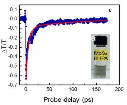
Ultrafast Intrinsic Photoresponse and Direct Evidence of Sub-Gap States in Liquid Phase Exfoliated MoS2 Thin Films2-Dimensional structures with swift optical response have several technological advantages, for example they could be used as components of ultrafast light modulators, photo-detectors, and optical switches. Here we report on the fast photo switching behavior of thin films of liquid phase exfoliated MoS2, when excited with a continuous laser of λ = 658 nm (E = 1.88 eV), over a broad range of laser power. Transient photo-conductivity measurements, using an optical pump and THz probe (OPTP), reveal that photo carrier decay follows a bi-exponential time dependence, with decay times of the order of picoseconds, indicating that the photo carrier recombination occurs via trap states. The nature of variation of photocurrent with temperature confirms that the trap states are continuously distributed within the mobility gap in these thin film of MoS2, and play a vital role in influencing the overall photo response. Our findings provide a fundamental understanding of the photo-physics associated with optically active 2D materials and are crucial for developing advanced optoelectronic devices.
|
|
References
- K. S. Novoselov, A. K. Geim, S. V. Morozov, D. Jiang, Y. Zhang, S. V. Dubonos, I. V. Grigorieva, and A. A. Firsov, Electric field effects in atomically thin carbon films, Science, 306 (5696), 666-669 (2004).
- A. K. Geim and K. S. Novoselov, The rise of graphene, Nature Mater., 6 (3), 183-191 (2007).
- K. F. Mak, C. Lee, J. Hone, J. Shan, and T. F. Heinz, Atomically thin MoS2: a new direct-gap semiconductor, Phys. Rev. Lett. 105, 136805 (2010).
- A. K. Geim and I. V. Grigorieva, Van der Waals heterostructures, Nature, 499, 419-425 (2013).
Page last updated on October 20, 2017 (CP/KMD).