

FY2021 Annual Report
Femtosecond Spectroscopy Unit
Associate Professor Keshav Dani

Abstract
In recent years, the ability to synthesize, engineer & observe low dimensional materials, with properties determined by variations on the nanometer length scale has led to novel phenomena and applications. On the other hand, modern lasers deliver powerful, ultrashort pulses of light allowing us to observe the interaction of electrons and atoms on the femtosecond timescale. Together, these technologies allow us to study new paradigms in light-matter interaction – with femtosecond temporal resolution and nanometer spatial resolution. In FY2021, Femtosecond Spectroscopy Unit has directed these broad capabilities towards four different areas of study:
- Energy Materials, where we study the ultrafast trapping dynamics at defect sites in perovskite photovoltaic materials.
- Terahertz Devices and Applications, where we develop array structures for the generation of engineered terahertz radiation.
- Low-dimensional materials and interfaces, where we study the electronic structure and dynamics in 2D semiconductors and metal-insulator or metal-semiconductor interfaces.
- Interdisciplinary research , – On Demand Drug Delivery, where we study the use of powerful ultrafast lasers to trigger controlled release in a drug delivery system.
1. Staff
- Dr. Keshav M. Dani, Professor
- Dr. Michael M. Man, Researcher
- Dr. Julien Madéo, Researcher
- Dr. Christopher E. Petoukhoff, Researcher
- Dr. Arka Karmakar, Researcher
- Dr. David Bacon, Researcher
- Dr. Abdullah Al Mahboob, Researcher
- Dr. Filchito Renee Bagsican, Researcher
- Dr. Jacques Hawecker, Researcher
- Dr. Viktoras Lisicovas, Junior Research Fellow
- Dr. Andrew Winchester, Graduate Student/Junior Research Fellow
- Dr. Joel Perez Urquizo, Graduate Student
- Vivek Pareek, Graduate Student
- Sofiia (Sonya) Kosar, Graduate Student
- Xing Zhu, Graduate Student
- Maria-Carla Lupu, Graduate Student
- Prajakta Kokate, Graduate Student
- Nicholas Chan, Technician
- Yumi Ito, Administrative Assistant
2. Collaborations
Theme: Energy Materials
Type of Collaboration: Joint Research
- Researchers:
- S. D. Stranks, Cavendish Laboratory, University of Cambridge, Cambridge, UK
- P. A. Midgley, Department of Materials Science and Metallurgy, University of Cambridge, Cambridge, UK
- J. S. Park, Department of Physics, Kyungpoook National University, Daegu, SOUTH KOREA
Theme: Terahertz Devices and Applications
Type of Collaboration: Joint Research
- Researchers:
- E. F. Miyamaru, Department of Physics, Shinshu University, Nagano, JAPAN
Theme: Low-Dimensional Materials and Interfaces
Type of Collaboration: Joint Research
- Researchers:
- K. Tanaka, Department of Physics, Kyoto University, Kyoto, JAPAN
- Xiaoquin (Elaine) Li, University of Texas at Austin, USA
- T. F. Heinz, Stanford University, California, USA
- T. Cao, University of Washington, Seattle, USA
- F. H. da Jornada, Department of Materials Science and Engineering, Stanford University, USA
- Y. Okada, Okinawa Inst. Of Science and Technology, JAPAN
- K. Watanabe, Research Center for Functional Materials, NIMS, Tsukuba, JAPAN
- T. Taniguci, International Center for Materials Nanoarchitectonics, NIMS, Tsukuba, JAPAN
Theme: Interdisciplinary Research – On-Demand Drug Delivery
Type of Collaboration: Joint Research
- Researchers:
- T. Nakano, Neurobiology Research Unit, Okinawa Inst. Of Science and Technology, JAPAN
- J. Wickens, Neurobiology Research Unit, Okinawa Inst. Of Science and Technology, JAPAN
3. Activities and Findings
3.1 Energy Materials
A. Unraveling the Varied Nature and Roles of Defects in Hybrid Halide Perovskites with Time-Resolved Photoemission Electron Microscopy
[Energy & Environmental Science 14, 6320 (2021)]
Hybrid halide perovskites have emerged as one of the most promising photovoltaic materials of the past decade. Perovskite solar cells now regularly output over 20 % of photo-conversion efficiency in single junction solar cells, and already exceeded 29 % in tandem devices. However, the presence of defects in hybrid perovskite thin films [1] has been detrimental to material properties, and has been a critical reason preventing devices from reaching their full potential [2]. Circumventing these detrimental effects requires understanding the nature of the defects that can occur, their role in performance losses and their stability under controlled operational conditions.
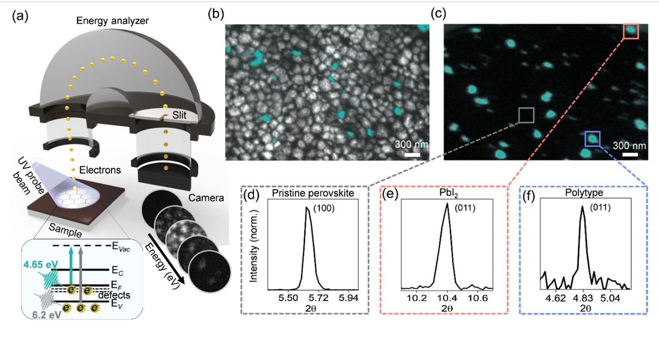
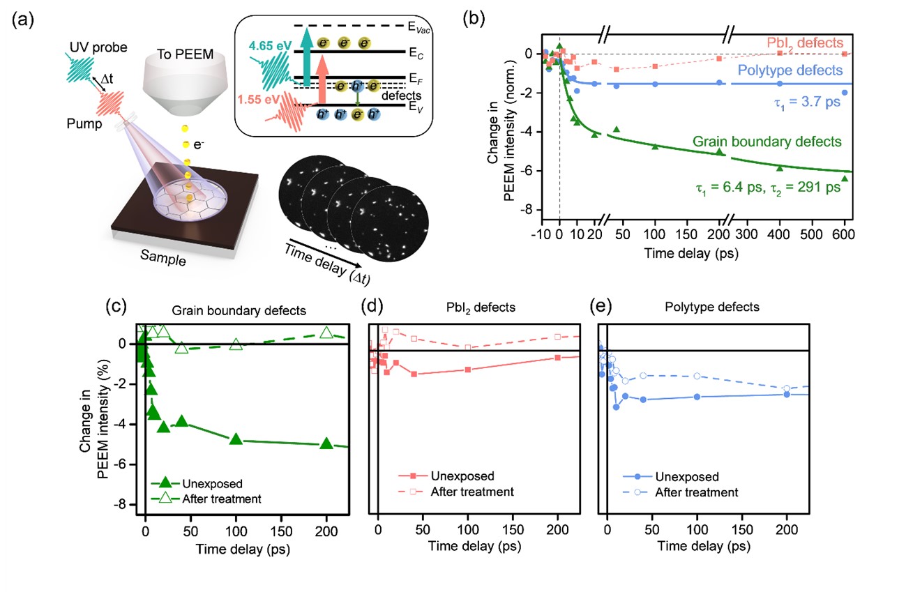
In this work, we have utilized photoemission electron spectro-microscopy (PEEM) [3] to directly image the nanoscale defects in state-of-the-art triple cation mixed halide perovskite thin films (Figure 1a). By combining PEEM with synchrotron based x-ray microscopies, we have uncovered the presence of multiple types of defects (Figure 1b-f). By employing time-resolved photoemission electron microscopy (TR-PEEM) [4] (Figure 2a), we found that depending on their nature, these defects played surprisingly varied roles in charge carrier trapping – from highly detrimental to relatively benign (Figure 2b). They also showed a varied response to passivation strategies [5] (Figure 2c-e). The presence of multiple types of defects, with varied roles in device performance and varied responses to passivation strategies, highlights the need to develop targeted approaches that address each type of defect and their detrimental impact.
References Section 3.1.A:
[1] J. Ball and A. Petrozza, Defects in perovskite-halides and their effects in solar cells, Nat. Energy 1, 16149 (2016).
[2] S. Stranks, Nonradiative losses in metal halide perovskites, ACS Energy Lett. 2, 1515 (2017).
[3] T. Doherty, A. Winchester, et al., Performance-limiting nanoscale trap clusters at grain junctions in halide perovskites, Nature 580, 360 (2020).
[4] M. Man, et al., Imaging the motion of electrons across semiconductor heterojunctions, Nature Nanotech. 12, 36 (2017).
[5] M. Anaya, et al., Origin of light-induced photophysical effects in organic metal halide perovskites in the presence of oxygen, J. Phys. Chem. Lett. 9, 14 (2018).
B. Nanoscale chemical heterogeneity dominates the optoelectronic response of alloyed perovskite solar cells
[Nature Nanotechnology 17, 190-196 (2022)]
Halide perovskites have recently seen tremendous success in photovoltaic applications, despite their heterogenous optoelectronic, chemical, and structural properties, which has been an ongoing paradox [1-3]. Here, we employed a combination of correlative nanoscale optical, structural, and compositional techniques to identify local regions of disorder that affect the optoelectronic response. Quantitative hyperspectral microscopy in conjunction with spatially-resolved photoluminescence on solution-processed mixed-cation [4], mixed-halide FA0.79MA0.16Cs0.05Pb(I0.83Br0.17)3 perovskite thin films revealed that regions of low photoluminescence quantum efficiency (PLQE) were correlated with regions of low quasi-Fermi level splitting (QFLS) and hence a lower implied open circuit voltage (Figure 1).
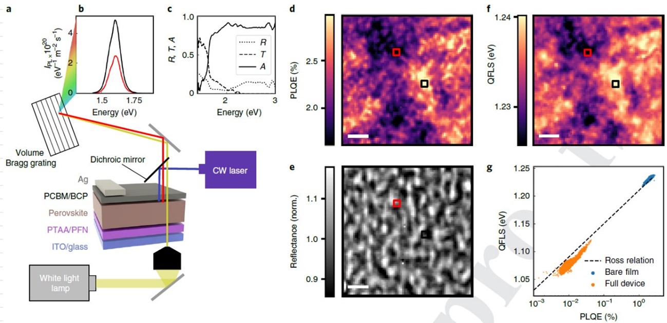
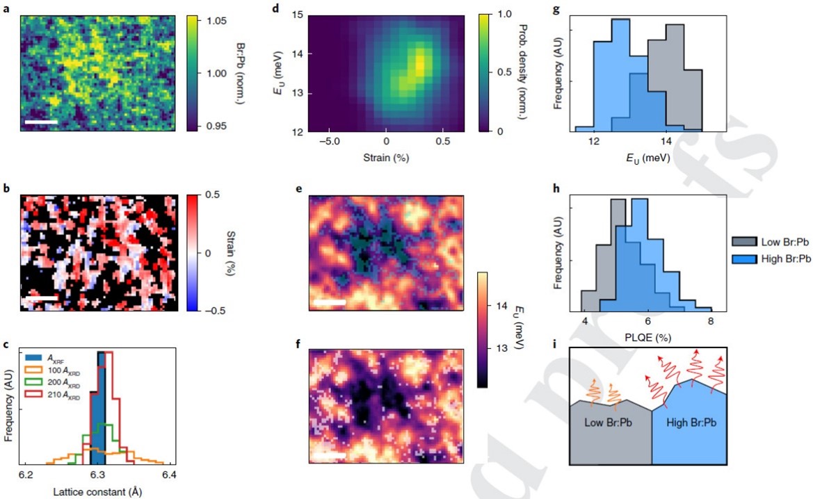
Using this methodology, we then calculated and compared the Urbach Energy (a measure of the crystalline disorder [5]) to nanoscale maps of the chemical composition and structure obtained from nano X-ray diffraction and fluorescence (nXRD and nXRF) measurements (Figure 2). This revealed that the higher Br:Pb regions exhibited the highest PLQE and lowest electronic disorder, despite the presence of a low-energy emission shoulder, which indicated disorder. Meanwhile, sites with low Br content contained deep trap states associated with non-radiative recombination and electronic disorder, which was identified by correlative photoemission electron microscopy (PEEM) measurements at OIST [3]. This apparent contradiction in the disorder of high Br content regions was explained through a charge-funneling phenomenon, which was verified using transient absorption microscopy. The higher Br content regions contain low-energy, ordered inclusions, which tend to collect free charge carriers. This funneling prevents the carriers from being captured by deep trap states located in low Br content regions, resulting in high luminescence yields and device performance. Thus, our work provides a nanoscale picture of how the energetic landscape of halide perovskites influences photodoping, carrier recombination, and trapping, as well as explaining the apparent defect tolerance of these materials.
References Section 3.1.B:
[1] J. Y. Kim, et al., Chem. Rev. 120, 7867–7918 (2020).
[2] E. M. Tennyson, et al., Nat. Rev. Mater. 4, 573–587 (2019).
[3] T. A. S. Doherty, et al., Nature 580, 360–366 (2020).
[4] M. Saliba, et al., Energy Environ. Sci. 9, 1989–1997 (2016).
[5] M. Ledinsky, et al., J. Phys. Chem. Lett. 10, 1368–1373 (2019).
3.2 Terahertz Devices and Applications
A. Photoconductive emitters for pulsed terahertz generation
[Journal of Optics, 23, 6, 1-29 (2021)]
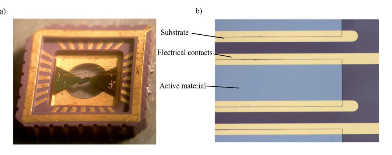
Conceived over 30 years ago, photoconductive (PC) emitters have proved essential in the development and spread of Terahertz (THz) technology [1]. Since then, it has undergone significant improvements in output power, conversion-efficiency, and bandwidth, all of which have led to its use in various spectroscopic and commercial imaging applications [2]–[4]. An image of a typically PC antenna is shown in Figure 1a. In its simplest form it consists of a semiconducting material with two metallic contacts, separated by the photoconductive gap. When the gap is illuminated by an ultrafast optical beam, free carriers are accelerated by a bias field applied between the electrical contacts resulting in pulsed THz emission. Its simplicity, ease of use, its reliability and relatively low cost have all led to its widespread use in almost every THz laboratory in the world.
In this review article, we provide an overview of the literature, highlighting the key milestones which has brought about the success of the PC antenna. After discussing the basic principles of THz emission, and its use in a THz time-domain spectroscopy setup, we examine the various improvements it has undergone since it was first realised. These include the numerous materials and antenna designs which have been proposed to improve its capabilities [5]–[8]. Next, we examine how large-scale PC array structures, depicted in Figure 1b, have proved a viable source of high-field THz radiation [9], [10]. We finish by looking forward to the future of the technology and examine how these devices can be adapted to work with high-power laser systems.
References Section 3.2.A:
[1] M. Tani et al., Emission characteristics of photoconductive antennas based on low-temperature-grown GaAs and semi-insulating GaAs, Appl. Opt. 36, 30, 7853 (1997).
[2] C. A. Schmuttenmaer, Exploring Dynamics in the Far-Infrared with Terahertz Spectroscopy, Chem. Rev. 104, 1759-1779 (2004).
[3] A. G. Davies et al., Terahertz spectroscopy of explosives and drugs, Mater. Today 11, 3, 18-26 (2008).
[4] R. M. Woodward et al., Terahertz Pulsed Imaging of Skin Cancer in the Time and Frequency Domain, J. Biol. Phys. 29, 257-261 (2003).
[5] D. R. Bacon et al., Free-space terahertz radiation from a LT-GaAs-on-quartz large-area photoconductive emitter, Opt. Express 24, 23, 26986 (Nov. 2016).
[6] R. B. Kohlhaas et al., 637 μ W emitted terahertz power from photoconductive antennas based on rhodium doped InGaAs, Appl. Phys. Lett. 117, 13, 3-7 (2020).
[7] J. Madéo et al., Ultrafast properties of femtosecond-laser-ablated GaAs and its application to terahertz optoelectronics, Opt. Lett. 40, 14, 3388 (2015).
[8] G. Matthäus et al., Microlens coupled interdigital photoconductive switch, Appl. Phys. Lett. 93, 9 (2008).
[9] D. R. Bacon et al., Photoconductive arrays on insulating substrates for high-field terahertz generation, Opt Express 28, 12, 17219-17231 (2020).
[10] X. Ropagnol et al., Intense THz Pulses with large ponderomotive potential generated from large aperture photoconductive antennas, Opt. Express 44, 11210, 83001-45016 (2016).
B. High Field Single- to Few-Cycle THz Generation with Lithium Niobate
[Photonics 08, 183 (2021)]
The transient Terahertz (THz) radiation, as a gap between traditional electronics and optics, has attracted enormous research interest due to its fascinating applications in physics, chemistry, and biology. In condensed matter physics, it has been widely used as a spectroscopic tool that provides a unique probe for low energy excitations such as lattice vibration [1], exciton transition [2], charge carrier motion [3], and spin excitation [4]. Recent advances in generation techniques have provided access to transient THz pulses with peak fields exceeding the MV/cm range using tabletop setups. This intense THz radiation has enabled new applications in the manipulation of matter over picosecond timescales [5]. Among various tabletop techniques, lithium niobate (LN) crystal shows unique advantages for generating high-field THz pulse with a narrow spectrum at relatively low frequencies.
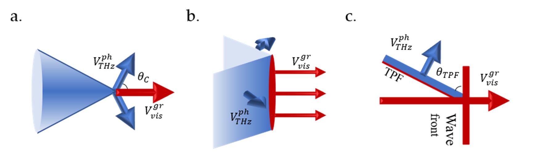
In this review, we focus on introducing single- to few-cycle THz generation in LN, including the basic principles, techniques, latest developments, and current limitations. First, we discuss the phase matching requirements of LN, which leads to Cherenkov-like radiation (Figure 1a, b), and the tilted pulse front (TPF) technique (Figure 1c). Particularly, we emphasize on the TPF technique, which has been shown to improve THz generation efficiency, but still has many limitations. Different geometries used to produce continuous and discrete TPF are systematically discussed. We summarize the advantages and limitations of current techniques and future trends.
References Section 3.2.B:
[1] Leguy, A. M. A., et al. Dynamic disorder, phonon lifetimes, and the assignment of modes to the vibrational spectra of methylammonium lead halide perovskites, Phys. Chem. Chem. Phys 18, 27051-27066 (2016).
[2] Steinleitner, P., et al. Direct Observation of Ultrafast Exciton Formation in a Monolayer of WSe2, Nano Lett 17, 1455-1460 (2017).
[3] La-o-vorakiat, C., et al. Elucidating the role of disorder and free-carrier recombination kinetics in CH3NH3PbI3 perovskite films, Nat. Commun 6, 7903 (2015).
[4] Yu, S., et al. High-Temperature Terahertz Optical Diode Effect without Magnetic Order in Polar FeZnMo3O8, Phys. Rev. Lett 120, 037601 (2018).
[5] Kozina, M., et al. Terahertz-driven phonon upconversion in SrTiO3, Nat. Phys 15, 387-392 (2019).
C. Ultrafast Frequency-Shift Dynamics at Temporal Boundary Induced by Structure-Dispersion Switching of Waveguides
[Physical Review Letters 127, 053902 (2021)]
Space-time phenomena have allowed the emergence of exotic physics such as broadband nonreciprocal applications [1] and Hawking radiation [2]. Among them, a temporal boundary, a time-domain counterpart of the spatial boundary, which can be established via a sudden change of material parameters, is considered a fundamental element. The frequency of a propagating wave can be abruptly shifted, while conserving incident wavenumber, when it propagates across a temporal boundary, breaking translational symmetry. This allows to achieve high frequency conversion efficiencies, even with weak signals [3].
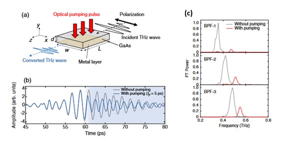
Here, we experimentally demonstrate the observation of frequency shift at a temporal boundary an its dynamics in the THz range. Our scheme relies on the control of the structural dispersion of a metal-semiconductor waveguide. The waveguide is photoexcited with an optical pump pulse while a THz pulse propagates in the waveguide (Fig.1 (a)) leading to ultrafast structural-dispersion switching at sub-picosecond timescales. We observe up to 23% conversion efficiency associated with a rapid variation of the THz frequency around the temporal boundary (Fig.1 (b) and (c)). Our approach opens a new avenue for efficient wavelength conversion in the THz range.
References Section 3.2.C:
[1] E. Galiffi, et al., Broadband nonreciprocal amplification in luminal metamaterials, Phys. Rev. Lett. 123, 206101 (2019).
[2] S. Weinfurtner, et al., Measurement of stimulated Hawking emission in an analogue system, Phys. Rev. Lett. 106, 021302 (2011).
[3] K. Lee, et al., Linear frequency conversion via sudden merging of meta-atoms in time-variant metasurfaces, Nat. Photonics 12, 765-773 (2018).
3.3 Low Dimensional Materials and Interfaces
A. Visualization of two-dimensional transition dipole moment texture in momentum space using high-harmonic generation spectroscopy
[Phys. Rev. B 103, L161406 (2021)]
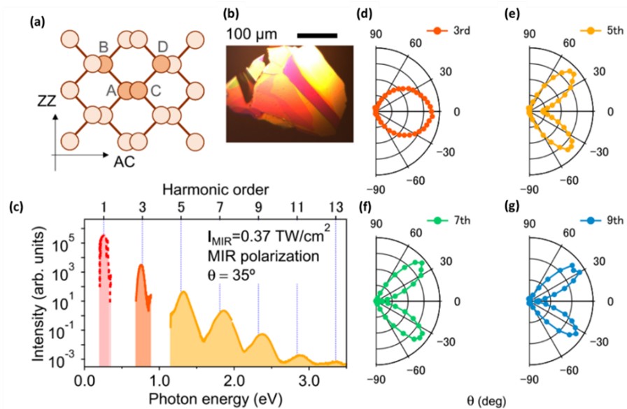
High-harmonic generation (HHG) in atomically thin materials is strikingly different from that in atomic gases [1,2], and it enables us to access electronic properties such as the band structure, Berry curvature, and valence electron density. Despite the differences, the HHG process in solids can be understood in the three-step model framework analogous to the gaseous media: 1) creation, 2) acceleration, and 3) recombination of electron hole pair. Creation and recombination of electron-hole pair originates from the interband polarization and is dictated by the transition dipole moment (TDM). Acceleration on the other hand induced an intraband current which provides information about the band structure of the material. Typically, HHG measurements have been carried out using intense light far off from the resonance of the band gap energy of the material. In this regime, it is difficult to separate out the relation between HHG and the TDM texture as several bands in the entire Brillouin zone get involved in the process. In this study we show that polarization-resolved HHG measurements with band-gap resonant excitation can be used to probe the transition dipole moment (TDM) texture in momentum space in two-dimensional semiconductors. We use bulk black phosphorus for our study as it offers a simple two-band system with anisotropic properties based on its crystal structure (see fig 1(a)). Using a mid-infrared (MIR) pump of 0.26 eV, we generate HHG in bulk BP up to 13th harmonic (see fig 1(c)). We also observed a unique crystal-orientation dependence of the HHG yields and polarizations for different harmonics (see fig 1(d-g)). Such pump arrangement allows us to map out the TDM texture related to the interatomic bonding structure. Our results show the potential of HHG to probe the electronic structure in solids.
References Section 3.3.A:
[1] Liu, H. et al., High-harmonic generation from an atomically thin semiconductor, Nat. Phys. 13, 262–265 (2016).
[2] Yoshikawa, N. et al., High-harmonic generation in graphene enhanced by elliptically polarized light excitation, Science 356, 736–738 (2017).
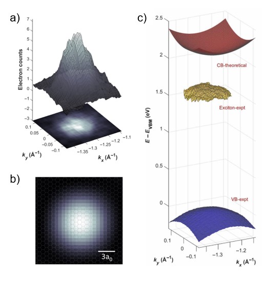
B. Experimental measurement of the intrinsic excitonic wave function
[Science Advances 7, eabg0192 (2021)]
An exciton, a two-body composite quasiparticle formed of an electron and hole, is a fundamental optical excitation in condensed matter systems. Theoretical description of excitons is naturally formulated in terms of the relative electron-hole coordinates, particularly for the Wannier-type excitons, where electron-hole separation extends over many lattice sites [1,2]. These descriptions, constituting the excitonic wave function in real space, analogous to the well-known wave functions describing the hydrogen atom, directly define the exciton’s size and shape. However, since its discovery nearly a century ago, a measurement of the excitonic wave function has remained beyond experimental reach.
Over the past decade, the discovery of robust excitons in two-dimensional systems and advances in angle-resolved photoemission spectroscopy (ARPES) techniques [4–6] have created opportunities for us to tackle this problem. In this work, we use time-resolved and spatial resolved ARPES technique pioneered in our laboratory [6] to directly image the excitonic wave function in reciprocal space. By measuring the momentum distribution of electrons photoemitted from excitons in monolayer WSe2, we obtained a direct visual of the electron distribution around the hole in an exciton, revealing its 1.4 nm radial shape delocalized over many lattice sites (Figure 1a,b). Furthermore, we confirm the elusive theoretical prediction that the photoemitted electron exhibits an inverted energy-momentum dispersion relationship reflecting the valence band where the partner hole remains, rather than that of conduction band states of the electron (Figure 1c).
References Section 3.3.B:
[1] J. Frenkel, On the transformation of light into heat in solids, Phys. Rev. 37, 17–44 (1931).
[2] G. H. Wannier, The structure of electronic excitation levels in insulating crystals, Phys. Rev. 52, 191–197 (1937).
[3] M. Puppin et al., Time- and angle-resolved photoemission spectroscopy of solids in the extreme ultraviolet at 500 kHz repetition rate, Rev. Sci. Instrum. 90, 023104 (2019).
[4] A. K. Mills et al., Cavity enhanced high harmonic generation for extreme ultraviolet time- and angle-resolved photoemission spectroscopy, Rev. Sci. Instrum. 90, 083001 (2019).
[5] K. Medjanik et al., Direct 3D mapping of the Fermi surface and Fermi velocity, Nat. Mater. 16, 615–621 (2017).
[6] J. Madéo et al., Directly visualizing the momentum-forbidden dark excitons and their dynamics in atomically thin semiconductors, Science 370, 1199–1204 (2020).
C. The 2021 ultrafast spectroscopic probes of condensed matter roadmap
[Journal of Physics: Condensed Matter 33, 353001 (2021)]
In the 60 years since the invention of the laser, the scientific community has developed numerous fields of research based on these bright, coherent light sources, including the areas of imaging, spectroscopy, materials processing and communications. Ultrafast spectroscopy and imaging techniques are at the forefront of research into the light–matter interaction at the shortest times accessible to experiments, ranging from a few attoseconds to nanoseconds. Light pulses provide a crucial probe of the dynamical motion of charges, spins, and atoms on picosecond, femtosecond, and down to attosecond timescales, none of which are accessible even with the fastest electronic devices. Furthermore, strong light pulses can drive materials into unusual phases, with exotic properties. This perspective article describes the current state-of-the-art in experimental and theoretical studies of condensed matter using ultrafast probes.
The specific contribution of the Femtosecond Spectroscopy Unit is in Section 9 – Time-resolved photoemission spectroscopies of 2D semiconductors and their heterostructures. In particular, we discuss the development of time-resolved photoemission electron microscopy (TR-PEEM) and time-resolved angle-resolved photoemission spectroscopy (TR-ARPES) to study 2D semiconductors. After a brief description of current capabilities, we describe the future challenges in the field.
D. Visualizing superconductivity in a doped Weyl semimetal with broken inversion symmetry
[Phys. Rev. B 104,115102 (2021)]
Weyl semimetals are three dimensional topological and gapless materials that hosts fermi arcs on the surface and Weyl cones in the bulk [1]. Weyl semimetals can host superconducting states as well which leads to exotic topological superconductivity [2]. This provides a possible direction to realize zero energy modes related to Majorana fermions which may be useful for quantum computation. Recently, the experimental discovery of edge supercurrent in MoTe2 has increased the interest in the material for the possible existence of topological superconducting phase [3]. The transition temperature for the superconducting phase in MoTe2 is below 0.1K at ambient pressure and can be enhanced to a few kelvin though chemical substitution. However, strong chemical substitution/doping can also prevent the structural transition from T to Td phase in the system which is important for observing Weyl semimetal state. Here, using scanning tunneling microscopy, we study an optimally doped MoTe1.85Se0.15 with bulk Tc close to 1.5K. We identify the existence of a low temperature Td phase through quasiparticle interference imaging and confirm the presence of global superconductivity in the sample (see figure 1). We also find that the superconducting coherence length is larger than the characteristic length scale of existing chemical disorder making the system a robust superconductor in the Weyl semimetal normal phase.
References Section 3.3.D:
[1] Xu, S.-Y. et al., TOPOLOGICAL MATTER. Discovery of a Weyl fermion semimetal and topological Fermi arcs, Science 349, 613–617 (2015).
[2] Hosur, P., et al., Time-reversal-invariant topological superconductivity in doped Weyl semimetals, Phys. Rev. B Condens. Matter 90, 045130 (2014).
[3] Wang, W. et al., Evidence for an edge supercurrent in the Weyl superconductor MoTe2, Science 368, 534–537 (2020).
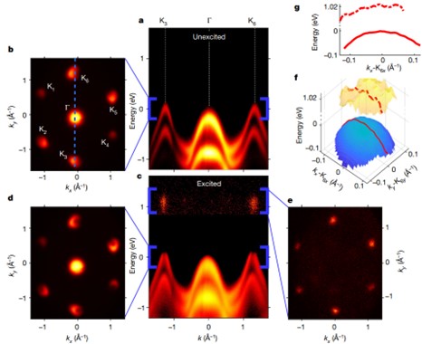
E. Structure of the moiré exciton captured by imaging its electron and hole
[Nature 603, 247-252 (2022)]
Heterostructures created by stacking two different van der Waals monolayer (1L) semiconductors such as transition metal dichalcogenides (TMDCs, e.g., MoS2) provide a path way to engineer novel materials with unique optoelectronic properties [1]. Recently, interlayer excitons (ILX) in hetero-bilayer systems have attracted great interest. ILXs are spatially separated bound electron hole pairs such that electrons present in one layer are bound to holes in another layer of the heterostructure by coulomb interaction. Such spatial separation results in the ILXs having long lifetimes which has made them an attractive platform to study many-body exciton physics as well as various device applications. On top of that the two 1L semiconductors in the heterostructure can be put together with a small twist angle between them, giving rise to moiré superlattices which modulates its electronic structure and can give rise to various novel phenomena such as superconductivity. However, a better understanding of various properties of ILXs such as its size, its valley configuration, and the effect of the moiré confinement is still largely missing. Several optical spectroscopic studies, performed on a variety of heterostructure systems, provide only partial information regarding the nature of ILXs[2]–[4]. For instance, optical studies can access only a limited portion of the momentum distribution of the ILX and thus cannot provide complete information about its size or its valley configuration reliably. One needs access to the full momentum space distribution of both of its bound electrons and holes for a complete understanding.
In this study, using Time-Resolved Angle Resolved Photoemission Spectroscopy (Tr-ARPES), we map out the full first Brillouin zone of the WSe2/MoS2 heterostructure with a 2° twist angle between them (see Fig 1(a, b)). We excite the system with 1.6 eV pump and probe the band structure by photoemitting electrons using XUV probe. We show the band structure of the system at 25ps time delay after the pump pulse in Fig 1(c, e). We clearly see the electron distribution of interlayer excitons around 1 eV at the K point confirming the direct band gap nature of the ILX in WSe2/MoS2 heterostructure. Strikingly, we also see the absence of electrons, i.e., holes in the valence band at the K point (see figure 1(c, d)). The ability to directly measure both the constituent electron and hole distribution of the ILXs allow us to determine some of its key properties such as its size compared to the moiré superlattice as well its confinement within the moiré potential. We find that even though the size of the ILX (5.2 nm) is comparable to the moiré superlattice size (6.1 nm), the ILX is well confined within the moiré potential. Until recently large moiré patters were understood to be crucial to confine ILXs. However, our result shows that even small-period moiré patters can successfully confine ILXs, which are uniform over large regions, allowing the realization of extended arrays of localized excitations for quantum technology.
References Section 3.3.E:
[1] P. Rivera et al., Interlayer valley excitons in heterobilayers of transition metal dichalcogenides, Nat. Nanotechnol. 13, 11, 1004-1015 (2018).
[2] K. Tran et al., Evidence for moiré excitons in van der Waals heterostructures, Nature 567, 7746, 71-75 (2019).
[3] K. L. Seyler et al., Signatures of moiré-trapped valley excitons in MoSe2/WSe2 heterobilayers, Nature 567, 7746, 66-70 (2019).
[4] O. Karni et al., Infrared Interlayer Exciton Emission in MoS2/WSe2 Heterostructures, Phys. Rev. Lett. 123, 24, 247402 (2019).
F. Dominating Interlayer Resonant Energy Transfer in Type-II 2D Heterostructure
[ACS Nano 2022,
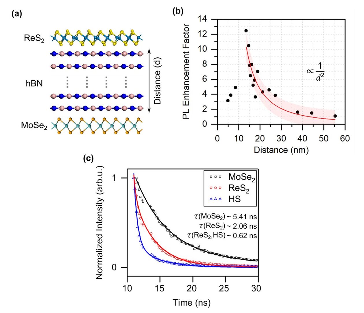
Type-II heterostructures (HSs) are integral part of modern-day electronics. Majority of the available layered transition metal dichalcogenide (TMD) materials form type-II HSs after vertically stacking them onto each other [1]. Upon photoexcitation interlayer charge (CT) and energy transfer (ET) are the two major carrier relaxation pathways in these HSs. Earlier reports [2,3] have shown that in the type-II TMD HSs interlayer CT is the main carrier relaxation pathway, which dominates over the interlayer ET process. In this work, we have shown that in a type-II HS formed between monolayers (1Ls) of molybdenum diselenide (MoSe2) and rhenium disulfide (ReS2) (Figure 1a), interlayer ET process dominates over the traditional CT process even without having any charge-blocking interlayer in between. This unusual dominating ET process results in 3.6 times enhanced photoluminescence (PL) emission from the HS area as compared to the 1L MoSe2 area alone (Figure 1b). After completely encapsulating the HS with hexagonal boron nitride (hBN) the enhancement factor was increased to 6.4.
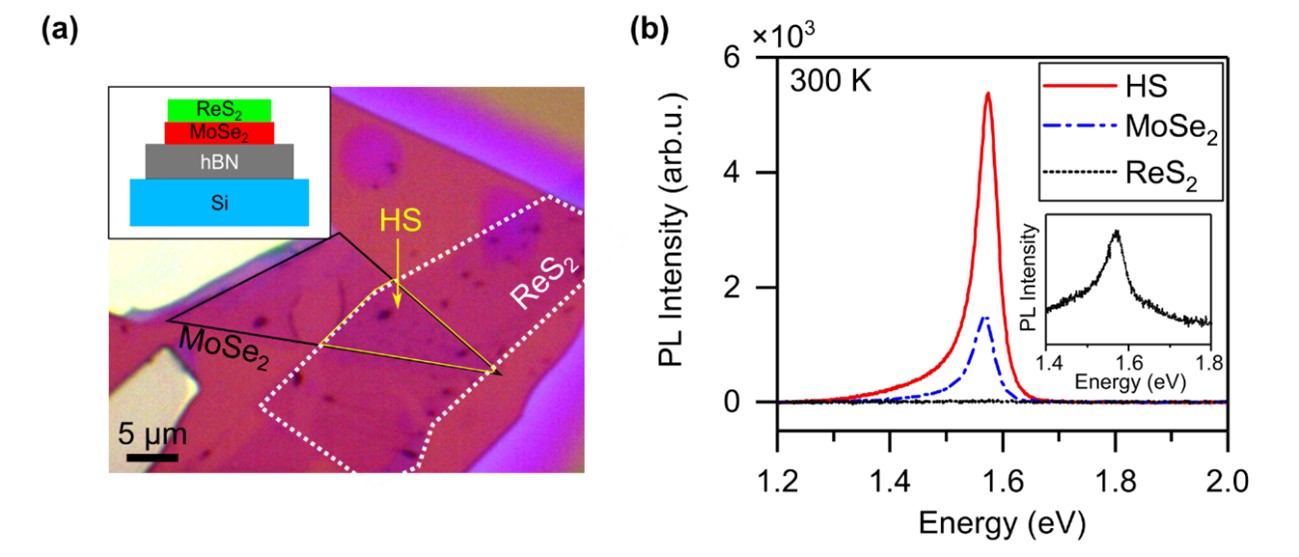
To check the distance (d) dependency in the reported ET process, we made several ReS2-MoSe2 HSs with varying hBN interlayer thicknesses (Figure 2a). Specifically, at a separation distance of 13.5 and 14.7 nm we achieved more than 1 order of magnitude higher PL emission from the HS area as compared to the 1L MoSe2 area, which then decreased with ~1/d2 dependency in our study (Figure 2b). The experimentally obtained 1/d2 dependency proves that 2D-to-2D transition dipole coupling dominates in our HSs [4].
References Section 3.3.F:
[1] Özçelik et al., Band alignment of two-dimensional semiconductors for designing heterostructures with momentum space matching, PRB 94, 035125 (2016).
[2] Ceballos et al., Ultrafast Charge Separation and Indirect Exciton Formation in a MoS2-MoSe2 van der Waals Heterostructure, ACS Nano 8, 12, 12717–12724 (2014).
[3] Peng et al., Ultrafast charge transfer in MoS2/WSe2 p–n Heterojunction, 2D Mater. 3, 025020 (2016).
[4] Barnes, W. L., Fluorescence near Interfaces: The Role of Photonic Mode Density, J. Mod. Opt. 45, 661−699 (1998).
3.4 Interdisciplinary Research
A. An On-Demand Drug Delivery System for Control of Epileptiform Seizures
[Pharmaceutics 14(2), 468 (2022)]
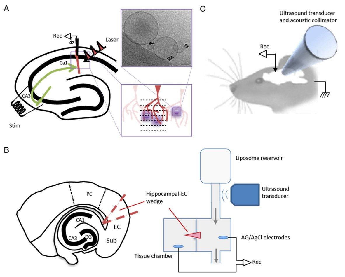
Drug delivery systems have the potential to deliver high concentrations of drug to target areas on demand, while elsewhere and at other times encapsulating the drug, to limit unwanted actions. Here, in collaboration with the Neurobiology Research Unit at OIST, we show proof of concept in vivo and ex vivo tests of a novel drug delivery system based on hollow-gold nanoparticles tethered to liposomes (HGN-liposomes), which become transiently permeable when activated by optical or acoustic stimulation. We show that laser or ultrasound simulation of HGN-liposomes loaded with the GABAA receptor agonist, muscimol, triggers rapid and repeatable release in a sufficient concentration to inhibit neurons and suppress seizure activity [Fig. 1]. In particular, laser-stimulated release of muscimol from previously injected HGN-liposomes caused subsecond hyperpolarizations of the membrane potential of hippocampal pyramidal neurons, measured by whole cell intracellular recordings with patch electrodes. In hippocampal slices and hippocampal–entorhinal cortical wedges, seizure activity was immediately suppressed by muscimol release from HGN-liposomes triggered by laser or ultrasound pulses. After intravenous injection of HGN-liposomes in whole anesthetized rats, ultrasound stimulation applied to the brain through the dura attenuated the seizure activity induced by pentylenetetrazol. Ultrasound alone, or HGN-liposomes without ultrasound stimulation, had no effect. Intracerebrally-injected HGN-liposomes containing kainic acid retained their contents for at least one week, without damage to surrounding tissue. Thus, we demonstrate the feasibility of precise temporal control over exposure of neurons to the drug, potentially enabling therapeutic effects without continuous exposure. For future application, studies on the pharmacokinetics, pharmacodynamics, and toxicity of HGN-liposomes and their constituents, together with improved methods of targeting, are needed, to determine the utility and safety of the technology in humans.
4. Publications
4.1 Journals
- K. Uchida, V. Pareek, K. Nagai, K. M. Dani, and K. Tanaka, Visualization of two-dimensional transition dipole moment texture in momentum space using high-harmonic generation spectroscopy,Physical Review B 103, L161406 (2021).
- M. K. L. Man†, J. Madéo†, C. Sahoo, K. Xie, M. Campbell, V. Pareek, A. Karmakar, E L. Wong, A. Al-Mahboob, N. S. Chan, D. R. Bacon, X. Zhu, M. M. M. Abdelrasoul, X. Li, T. F. Heinz, F. H. da Jornada, T. Cao, and K. M. Dani, Experimental measurement of the intrinsic excitonic wave function,Science Advances 7 (17), eabg0192 (2021).
- D. R. Bacon, J. Madéo and K. M. Dani, Photoconductive emitters for pulsed terahertz generation,Journal of Optics 23 (6), 064001 (2021).
- X. Zhu, D. R. Bacon, J. Madéo and K. M. Dani, High field single- to few-cycle THz generation with lithium niobate,Photonics 8 (6), 183 (2021).
- J. Lloyd-Hughes, P. M. Oppeneer, T. Pereira dos Santos, A. Schleife, S. Meng, M. A. Sentef, M. Ruggenthaler, A. Rubio, I. Radu, M. Murnane, X. Shi, H. Kapteyn, B. Stadtmüller, K. M. Dani, F. H. da Jornada, E. Prinz, M. Aeschlimann, R. L. Milot, M. Burdanova, J. Boland, T. Cocker and F. Hegmann, The 2021 ultrafast spectroscopic probes of condensed matter roadmapJ. Phys.: Condens.Matter 33 353001 (2021).
- F. Miyamaru, C. Mizuo, T. Nakanishi, Y. Nakata, KI. Hasebe, S. Nagase, Y. Matsubara, Y. Goto, J. Perez-Urquizo, J. Madeo and K. M. Dani, Ultrafast frequency-shift dynamics at temporal boundary induced by structural-dispersion switching of waveguides,Phys. Rev. Lett. 127 (5), 053902 (2021).
- Z. Wang, J. Olivares, H. Namiki, V. Pareek, K. M. Dani, T. Sasagawa, V. Madhavan and Y. Okada, Visualizing superconductivity in a doped Weyl semimetal with broken inversion symmetry,Phys. Rev. B 104 (11), 115102 (2021).
- S. Kosar, A. J. Winchester, T. A. S. Doherty, S. Macpherson, C. E. Petoukhoff, K. Frohna, M. Anaya, N. S. Chan, J. Madéo, M. K. L. Man, S. D. Stranks and K. M. Dani, Unraveling the varied nature and roles of defects in hybrid halide perovskites with time-resolved photoemission electron microscopy,Energy Environ. Sci. 14, 6320-6328 (2021).
- K. Frohna, M. Anaya, S. Macpherson, J. Sung, T. A. S. Doherty, Y. H. Chiang, A. J. Winchester, K. W. P. Orr, J. E. Parker, P. D. Quinn, K. M. Dani, A. Rao and S. D. Stranks, Nanoscale chemical heterogeneity dominates the optoelectronic response of alloyed perovskite solar cells,Nat. Nanotechnol. 17, 190-196 (2022).
- T. Nakano, S. B. Rizwan, D. M. A. Myint, J. Gray, S. M. Mackay, P. Harris, C. G. Perk, B. I. Hyland, R. Empson, E. W. Tan, K. M. Dani, J. N. Reynolds, J. R. Wickens, An on-demand drug delivery system for control of epileptiform seizures,Pharmaceutics 14, 468 (2022).
- O. Karni, E. Barré, V. Pareek, J. D. Georgaras, M. K. L. Man, C. Sahoo, D. R. Bacon, X. Zhu, H. B. Ribeiro, A. L. O’Beirne, J. Hu, A. Al-Mahboob, M. M. M. Abdelrasoul, N. S. Chan, A. Karmakar, A. J. Winchester, B. Kim, K. Watanabe, T. Taniguchi, K. Barmak, J. Madéo, F. H. da Jornada, T. F. Heinz and K. M. Dani, Structure of the moire exciton captured by imaging its electron and hole, Nature 603, 247-252 (2022)
- A. Karmakar, A. Al-Mahboob, C. E. Petoukhoff, O. Kravchyna, N. S. Chan, T. Taniguchi, K. Watanabe, and K. M. Dani, Dominating interlayer resnant energy transfer in type-II 2D heterostructure, ACS Nano Article ASAP (2022)
4.2 Books and other one-time publications
Nothing to report.
4.3 Oral and Poster Presentations
- Dani, K.M., Probing the dark side of the exciton with time-resolved ARPES, Quantum Materials and Devices Seminar, Invited Talk, Harvard University, MA, USA, Apr 7 (2021)
- Kosar, S., Winchester, A., Macpherson, S., Petoukhoff, C. E., Madéo, J., Man, M. K. L., Stranks, S. D., Dani, K. M., Investigation of Heterogeneous Charge Trapping Dynamics at Nanoscale Defects in Triple Cation Mixed Halide Perovskite Thin Films, 2021 Virtual MRS Spring Meeting & Exhibit, Oral Presentation (online), USA, Apr 17-23 (2021)
- Madéo, J., Man, M. K. L., Sahoo, C., Campbell, M., Pareek, V., Wong, E.L., Chan, N. S., Karmakar, A., Al-Mahboob, A., Mariserla, B. K. M., Li, X., Heinz, T.F., Cao, T., Dani, K. M., Time-resolved ARPES of excitons in a 2D semiconductor, Oral Presentation (online), CLEO 2021, San Jose, CA, USA, May 09-14 (2021)
- Man, M. K. L., Madéo, J., Sahoo, C., Xie, K., Campbell, M., Pareek, V., Karmakar, A., Wong, E. L., Al-Mahboob, A., Li, X., Heinz, T. F., Da Jornada, F. H., Cao, T., Dani, K. M., Directly visualization of excitonic wavefunction in 2D semiconductors by angle resolved photoemission spectroscopy, Oral Presentation (online), CLEO 2021, San Jose, CA, USA, May 09-14 (2021)
- Dani, K. M., Time Resolved ARPES of excitons in monolayer WSe2- the dark side of the exciton and the traumatic sudden separation, International Ultrafast Knowledge Coffee House, Seminar (online), PA, USA, May 03 (2021)
- Dani, K. M., Using Time-Resolved XUV ARPES To Probe Excitons, Chez Pierre Condensed Matt. Physics Seminar, Invited Talk (online), Massachusetts Institute of Technology, MA, USA, May 17 (2021)
- Dani, K. M.,Visualizing Dark Exciton Wavefunctions with Ultrafast μ-ARPES, Hot Topics in Ultrafast Science, Ultrafast Optical Phenomena Technical Group, OSA, Invited Talk, USA, Jun 15 (2021)
- Madéo, J.,Patch antennas for THz emission, Invited talk (online), 10th International symposium on ultrafast phenomena and Terahertz waves (ISUPTW2021), Chengdu, China, Jun 16-19 (2021)
- Dani, K. M.,Time-resolved ARPES of Excitons, OIST-HUJI Joint Research Initiative workshop, Seminar (online), OIST, Okinawa, Japan, Jul 13(2021)
- Pérez-Urquizo, J., Madéo, J., Dani, K. M., Optical losses in THz arrays of patch-antenna microcavities coupled to subwavelength wires, Invited talk (online), Terahertz Emitters, Receivers and Applications XII, San Diego, CA, USA, Aug 01-05 (2021)
- Dani, K. M., Probing the momentum coordinate of excitons using time-resolved ARPES, Invited Talk, SPIE, Spintronics XIV, San Diego, CA, USA, Aug 21-25 (2021)
- Dani, K. M., Imaging excitonic states with time-resolved photoemission spectroscopy in 2D semiconductor heterostructures, Invited talk (online), ASOMEA-X, University of Tokyo, Chiba, Japan, Oct 25-28(2021)
- Dani, K. M., Imaging excitonic states with time- and angle- resolved photoemission spectroscopy in 2D semiconductors, Material Science/CMP online seminar, Tor Vergata University, Rome, Italy, Oct (2021)
- Dani, K. M., Imaging the internal structure of the exciton, Invited Talk, VCS Seminar, Tata Institute of Fundamental Research (TIFR), Hyderabad, India, Nov (2021)
- Karmakar, A., Al-Mahboob, Petoukhoff, C. E., Kravchyna, O., Chan, N. S., Taniguchi, T., Watanabe, K., Dani, K. M., Dominating Interlayer Resonant Energy Transfer in Type-II 2D Heterostructures, Oral Presentation, 2021 MRS Fall Meeting & Exhibit, Boston, MA, USA, Nov 29- Dec 02 (2021)
- Dani, K. M. Time-resolved ARPES studies of 2D semiconductor heterostructures, Invited talk (online), The 12th International Conference on Advanced Materials and Devices (ICAMD) 2021, Jeju, S Korea, Dec 6-9 (2021)
- Dani, K. M. Exploring excitonic excitations through their momentum coordinates, Invited talk (online), Exciton Dynamics in Functional Materials, CECAM, Switzerland, Dec 13-16 (2021)
- Dani, K. M. Peering into the exciton, Invited Seminar (online), Department of Chemistry, University College London, UK, Jan 19 (2022)
- Kosar, S., Winchester, A. J., Doherty, T. A. S., Macpherson, S., Petoukhoff, C. E., Frohna, K., Anaya, M., Chan, N. S., Madéo, J., Man, M. K. L., Stranks, S. D., Dani, K. M., Exploring defects in triple cation mixed halide perovskite thin films using time-resolved photoemission electron microscopy, Oral Presentation (online), NanoGe Spring Meeting 2022, Spain, Mar 07-11 (2022)
- Dani, K. M., Understanding the role of nanoscale defect clusters in hybrid perovskite photovoltaics with time-resolved photoemission electron microscopy, Invited talk (online), NanoGe Spring Meeting 2022, Malaga, Spain, Mar 07-11 (2022)
- Dani, K. M.,Exploring Excitonic Excitations in Momentum Space, Invited talk (online), International Symposia on Creation of Advanced Photonic and Electronic Devices 2022 and Advanced Quantum Technology for Future 2022 (online), Kyoto University, Kyoto, Japan, March 8th (2022)
- Karmakar, A., Al-Mahboob, Petoukhoff, C. E., Kravchyna, O., Chan, N. S., Taniguchi, T., Watanabe, K., Dani, K. M., Resonant Energy Transfer in Type-II TMD Heterostructure, Oral Presentation (online), APS March Meeting 2022, Chicago, IL, USA, Mar 14-18 (2022)
- Bacon, D., Zhu, X., Pareek, V., Pérez-Urquizo, J., Chan, N. S., Bussolotti, F., Watanabe, K., Taniguchi, T., Man, M. K. L., Madéo, J., Goh, K. E. J., Dani, K. M., Study of momentum-resolved exciton dynamics in Monolayer Tungsten Disulfide, Oral Presentation, APS March Meeting 2022, Chicago, IL, USA, Mar 14-18 (2022)
- Dani, K. M.,Tracing the dynamics of excitons using time-and angle-resolved photoemission spectroscopy, Invited Talk, APS March Meeting 2022, Chicago, IL, USA, Mar 14-18 (2022)
- Dani, K. M.,Imaging the internal particles of excitons in 2D semiconductors, Invited talk (online), The Physical Society of Japan 2022 Annual (77th) Meeting, Tokyo, Japan, Mar 15-19 (2022)
5. Intellectual Property Rights and Other Specific Achievements
Nothing to report.
6. Meetings and Events
6.1 Seminar
Nothing to report.
6.2 Workshop
Nothing to report.
7. Other
Nothing to report.