

FY2020 Annual Report
Femtosecond Spectroscopy Unit
Associate Professor Keshav Dani

Abstract
In recent years, the ability to synthesize, engineer & observe low dimensional materials, with properties determined by variations on the nanometer length scale has led to novel phenomena and applications. On the other hand, modern lasers deliver powerful, ultrashort pulses of light allowing us to observe the interaction of electrons and atoms on the femtosecond timescale. Together, these technologies allow us to study new paradigms in light-matter interaction – with femtosecond temporal resolution and nanometer spatial resolution. In FY2020, Femtosecond Spectroscopy Unit has directed these broad capabilities towards three different areas of study:
- Energy Materials, where we study the ultrafast trapping dynamics at defect sites in perovskite photovoltaic materials.
- Terahertz Devices and Applications, where we develop array structures for the generation of engineered terahertz radiation.
- Low-dimensional materials and interfaces, where we study the electronic structure and dynamics in 2D semiconductors and metal-insulator/semiconductor interfaces.
1. Staff
- Dr. Keshav M. Dani, Professor
- Dr. Michael M. Man, Researcher
- Dr. Julien Madéo, Researcher
- Dr. Christopher E. Petoukhoff, Researcher
- Dr. Arka Karmakar, Researcher
- Dr. David Bacon, Researcher
- Dr. Abdullah Al Mahboob, Researcher
- Dr. Chakradhar Sahoo, Researcher
- Dr. Viktoras Lisicovas, Junior Research Fellow
- Dr. Andrew Winchester, Graduate Student/Junior Research Fellow
- Joel Perez Urquizo, Graduate Student
- Vivek Pareek, Graduate Student
- Sofiia (Sonya) Kosar, Graduate Student
- Xing Zhu, Graduate Student
- Dr. Oksana Kravchyna, Technician
- Nicholas Chan, Technician
- Yumi Ito, Administrative Assistant
2. Collaborations
Theme: Energy Materials
Type of Collaboration: Joint Research
- Researchers:
- S. D. Stranks, Cavendish Laboratory, University of Cambridge, Cambridge, UK
- P. A. Midgley, Department of Materials Science and Metallurgy, University of Cambridge, Cambridge, UK
- J. S. Park, Department of Physics, Kyungpoook National University, Daegu, South Korea
Theme: Terahertz Devices and Applications
Type of Collaboration: Joint Research
- Researchers:
- E. H. Linfield, University of Leeds, UK
- J. R. Freeman, University of Leeds, UK
- A. G. Davies, University of Leeds, UK
- L. Li, University of Leeds, UK
- Y. Todorov, CNRS, Sorbonne Universite, Paris, France
- C. Sirtori, CNRS, Sorbonne Universite, Paris, France
Theme: Low-Dimensional Materials and Interfaces
Type of Collaboration: Joint Research
- Researchers:
- C. Monney, Universite de Fribourg, Switzerland
- D. M. O’Carroll, Rutgers University, New Jersey, USA
- X. Li, University of Texas at Austin, USA
- T. F. Heinz, Stanford University, California, USA
- T. Cao, University of Washington, Seattle, USA
3. Activities and Findings
3.1 Energy Materials
A. Performance-Limiting Nanoscale Trap Clusters at Grain Junctions in Halide Perovskites
[Nature 580, 360-366 (2020)]
Hybrid organic-inorganic perovskites (HOIP) are an emerging material for applications in low-cost photovoltaic devices. Despite the rapid development of HOIP solar cell devices with record efficiencies exceeding 25% [1, 2], there are still ongoing efforts to reach the theoretical efficiency limits, which requires fundamental understanding of the sub-bandgap non-radiative trap states which lead to undesired charge carrier losses [3, 4]. Further, it is known that non-radiative losses and other detrimental effects such as strain and halide segregation can occur on sub-micrometer length scales, suggesting that the underlying trap clusters responsible could be very local in nature [4-7].
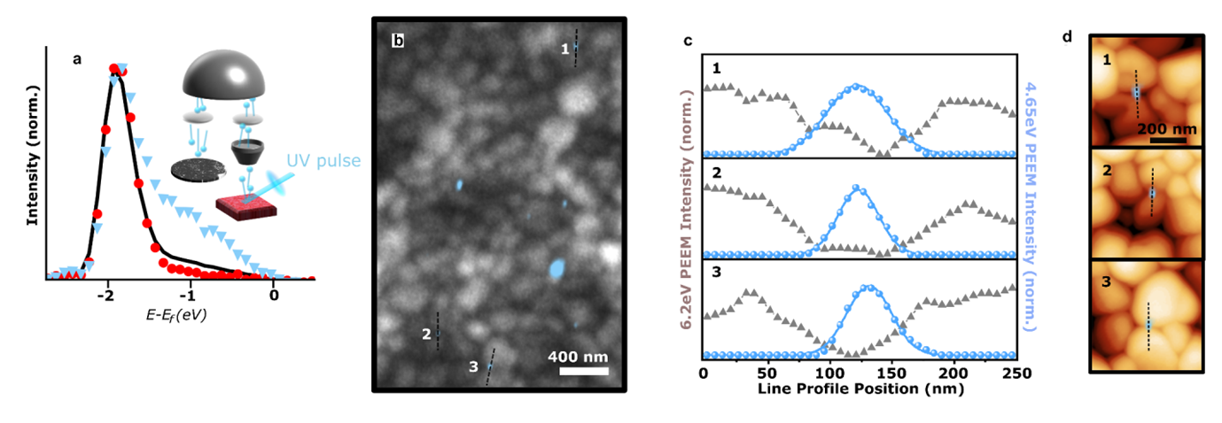
In this work, we use photoemission electron microscopy (PEEM) [8] to show for the first time the nanoscale presence and distribution of trap clusters in a mixed-cation mixed-halide HOIP films. We observe that there are local nanoscale regions which display a high density of mid-gap trap states (Figure 1a blue triangles) compared to other regions (Figure 1a red dots) or the spatially averaged response (Figure 1a black line). We find that these locations contain nanoscale clusters of traps (Figure 1b blue spots), which occur primarily at junctions between particular material grains (Figure 1b-d), where one grain is distorted structurally and compositionally, as revealed through correlated scanning electron diffraction (SED) microscopy and scanning transmission electron microscopy (STEM-EDX) measurements. We then studied the effect of these trap clusters on carrier recombination in the film. From regions of low photoluminescence (PL) yield (Figure 2a), we measure the subsequent trapping dynamics at these trap clusters using time-resolved PEEM [8] measurements (Figure 2b). We find that there is hole carrier trapping (Figure 2c) which happens only at the nanoscale trap clusters (Figure 2d) and not at other locations. By analyzing the trapping kinetics from many trap clusters simultaneously, we find that the trapping dynamics are consistent with a diffusion-limited trapping process. Our observations and results on trap sites in HOIP materials provide new nanoscale information which will better direct further investigations into understanding more fundamental properties of how these trap clusters form and affect device properties. These results have important implications for engineering future HOIP materials to prevent, isolate, or better-tolerate traps, which will lead to more efficient devices.

References:
[1] Jiang, Q. et al. Surface passivation of perovskite film for efficient solar cells. Nature Photonics 1 (2019).
[2] Best Research-Cell Efficiency Chart | Photovoltaic Research | NREL. https://www.nrel.gov/pv/cell-efficiency.html.
[3] Hörantner, M. T. et al. The Potential of Multijunction Perovskite Solar Cells. ACS Energy Lett. 2, 2506–2513 (2017).
[4] deQuilettes, D. W. et al. Impact of microstructure on local carrier lifetime in perovskite solar cells. Science 348, 683–686 (2015).
[5] Knight, A. J. et al. Electronic Traps and Phase Segregation in Lead Mixed-Halide Perovskite. ACS Energy Lett. 4, 75–84 (2019).
[6] Jones, T. W. et al. Lattice strain causes non-radiative losses in halide perovskites. Energy Environ. Sci. 12, 596–606 (2019).
[7] Zhao, J. et al. Strained hybrid perovskite thin films and their impact on the intrinsic stability of perovskite solar cells. Science Advances 3, eaao5616 (2017).
[8] Man, M. K. L. et al. Imaging the motion of electrons across semiconductor heterojunctions. Nature Nanotechnology 12, 36–40 (2017).
3.2 Terahertz Devices and Applications
A. Monolithic Patch-Antenna THz Lasers with Extremely Low Beam Divergence and Polarization Control
[ACS Photonics 2021, 8, 2, 412–417]
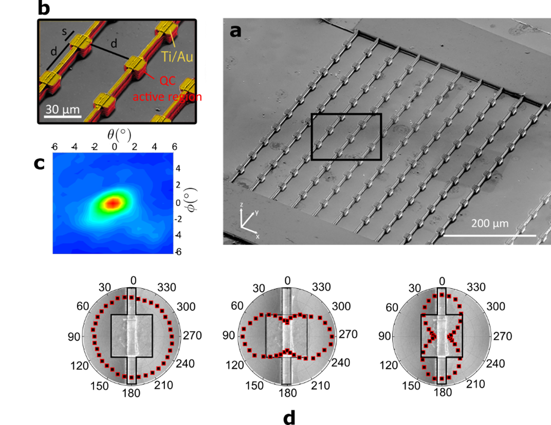
Arrays of patch antennas have impacted modern telecommunications in the RF range significantly, owing to their versatility in tailoring the properties of the emitted radiation such as beam width and polarization, along with their ease of fabrication. At higher frequencies, in the terahertz (THz) range, there exists a pressing need for a similar monolithic platform to realize and enable the advanced functionalities available in RF technology. This platform would benefit a wide variety of fields such as astronomy, spectroscopy, wireless communications, and imaging. In this work, we demonstrate THz lasers made of planar arrays of 10 X 10 patch antenna microcavities containing quantum cascade active semiconductor heterostructures that provide up to 25 mW output power with robust single mode frequency and spatial mode. This device architecture leads to an unprecedented beam divergence better than 2°x2° and radiates with any desired coherent polarization state. By interconnecting the symmetric square microcavities with narrow plasmonic wires along one direction, we introduce an asymmetry into the originally degenerate and cross-polarized TM01 and TM10 modes, leading to a precise control of the resonant frequency detuning between the TM modes. This feature allows to design devices radiating with any polarization from linear to circular. Our platform provides a solution to finally achieve monolithic terahertz emitters with integrated capabilities which could pave the way towards achieving a long-standing goal to transfer the advanced RF functionalities to the THz range.
B. Photoconductive arrays on insulating substrates for high-field terahertz generation
[Optics Express 28.12 (2020): 17219-17231]
Applications of high-field Terahertz (THz) pulses are diverse and include the ability to ionize Rydberg states in Na atoms, to vary superconductivity through the breakup of cooper pairs in YBa2Cu3O7 and to manipulate and control electron spin in antiferromagnets. The high THz fields required for these experiments, have typically been generated using table-top systems through optical rectification (OR) [1], two-colour air-plasma [2]. However, an alternative method is through the use of large-area photoconductive antennas (LAPCA) [3], [4], which produces THz radiation through the generation and acceleration of electron-hole pairs in semiconducting materials. Despite well documented saturation and heating effects, PC emission has several advantages over OR including a bias controllable output field and electrically switchable polarisation, while not requiring high-cost fragile non-linear crystals.
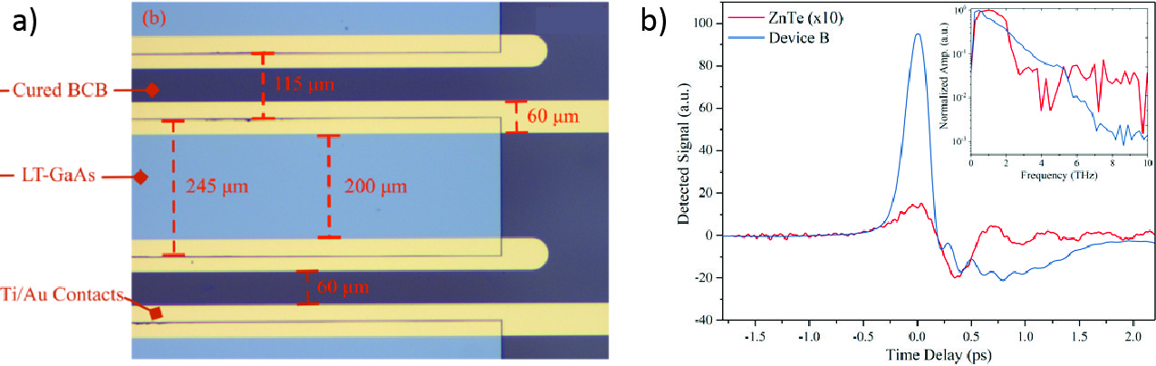
In this work we report on the design, fabrication and characterisation of large-area photoconductive THz array structures, consisting of a thin LT- GaAs active region transferred to an insulating substrate using a unique bonding process. The success of this fabrication process allowed the creation of 1.8x1.8cm2 array structure (pictured in Figure 4 with full dimensions in the caption). The electrically insulating, transparent substrate reduces the parasitic currents in the devices, allowing peak THz-fields as high as 120 kV/cm to be generated over a bandwidth >5 THz. These results are achieved using lower pulse energies than demanded by conventional photoconductive arrays and other popular methods of generating high-field THz radiation. Furthermore, when the emission properties are compared directed with OR with a ZnTe crystal, we obverse optical-to-THz conversion efficiencies 3 orders-of-magnitude greater using the array structure. The significant difference in emission properties of these two methods is highlighted in Figure 4b below.
References:
[1] K.-L. Yeh, M. C. Hoffmann, J. Hebling, and K. A. Nelson, “Generation of 10uJ ultrashort terahertz pulses by optical rectification,” Appl. Phys. Lett, vol. 90, p. 171121, 2007.
[2] T. I. Oh, Y. J. Yoo, Y. S. You, and K. Y. Kim, “Generation of strong terahertz fields exceeding 8 MV/cm at 1 kHz and real-time beam profiling,” Appl. Phys. Lett, vol. 105, p. 41103, 2014.
[3] D. H. Auston, A. M. Johnson, P. R. Smith, and J. C. Bean, “Picosecond optoelectronic detection, sampling, and correlation measurements in amorphous semiconductors,” Appl. Phys. Lett., vol. 37, no. 4, pp. 371–373, 1980.
[4] S. Winnerl, “Scalable microstructured photoconductive terahertz emitters,” J. Infrared, Millimeter, Terahertz Waves, vol. 33, no. 4, pp. 431–454, 2012.
3.3 Low-Dimensional Materials and Interfaces
A. Directly visualizing the momentum forbidden dark excitons and their dynamics in atomically thin semiconductors
[Science 370 (6521), 1199-1204 (2020)]
The unique optical properties of two-dimensional semiconductors, such as monolayer transition metal dichalcogenides, have provided deep insights into fundamental materials research and emerging nanotechnologies [1,2]. The strong Coulomb interactions and distinct structural symmetries in these materials give rise to a rich variety of photoexcited states, including bright and dark excitonic complexes that are tightly bound and valley-spin polarized [3]. However, directly accessing both bright and momentum-forbidden dark excitons and fully capturing their relaxation processes, occurring rapidly along both the energy and momentum axes, has not been possible with conventional experimental probes. In particular, a direct determination of the quasi-equilibrium exciton distribution over the entire Brillouin zone after the initial cooling is essential for future research and optoelectronic applications of two-dimensional materials. Here, by performing time- and momentum-resolved photoemission spectroscopy based on table-top MHz XUV source (21.7 eV) on a micron-scale monolayer flake of WSe2, we directly observe the exciton distribution at the K- and Q-valleys and measure their dynamics and relaxation pathways under different excitation conditions across the Brillouin zone.
In Figure 5, we present the ARPES data (K’-Γ-K cut) corresponding to the single particle bandstructure of WSe2 monolayer without optical pump (Figure 1a) and after photoexcitation with a 1.72 eV pump in resonance with the A exciton. The later shows the presence of two nearly degenerate excitonic states, with electrons at the K- and Q-valley respectively at an energy of ~1.72 eV above the valence band maximum.
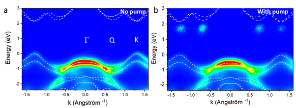
These excitons are characterized by multiple near-degenerate species involving holes in the K-valley and electrons in both the K- and Q-valleys of the Brillouin zone, with relaxation pathways dictated by the initial excitation conditions. For resonant excitation, we see the rapid formation of K-valley excitons, followed by scattering of the exciton population to the Q -valley in 400 fs In contrast, for above-gap excitation at 2.5 eV, we observe excitons forming within 500 fs, with electrons in the K- and Q-valley, but with a larger initial density at Q, and net scattering from the Q- to K-valley. Surprisingly, we also find that momentum-forbidden excitons dominate the quasi-equilibrium distribution. Our measurements provide the first global view of the ultrafast optical response of 2D semiconductors and demonstrate the impact of studying excited-state dynamics over the full Brillouin zone in condensed matter systems.
References:
[1] A. Pulickel et al., Two-dimensional van der Waals materials, Physics Today 69, 9, 38 (2016)
[2] Q. H. Wang et al., Electronics and optoelectronics of two-dimensional transition metal dichalcogenides, Nat. Nanotechnol. 7, 699 (2012).
[3] G. Wang et al., Excitons in atomically thin transition metal dichalcogenides, Rev. Mod. Phys. 90, 021001 (2018)
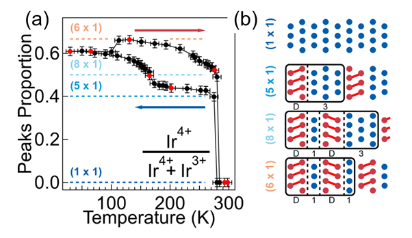
B. Examining the surface phase diagram of IrTe2 with photoemission
[Physical Review B 101, 235120 (2020)]
In transition metal dichalcogenide IrTe2, low-temperature charge-ordered phase transitions involving Ir dimers lead to the occurrence of stripe phases of different periodicities, and nearly degenerate energies [1-3]. Here, we carried out a detailed and systematic studies of the temperature dependent charge-ordered phases of IrTe2 with ARPES and XPS. We revealed that the first-order phase transition at Tc3 = 165 K is related to the (6 × 1) stripes phase, previously proposed to be the surface ground state.
Using XPS, we measure the evolution of the Ir dimer density upon cooling down to 30 K and warming back to room temperature by quantifying the Ir 4f core level peak intensities. While we confirm the sharp first-order transition occurring at Tc1, we observe a more intricate behavior below Tc2 at the surface. The (5 × 1) phase is replaced by the (8 × 1) phase that progressively changes into the (6 × 1) phase, indicating (6 × 1) domain growth at the expense of the (8 × 1) domains. However, our ARPES measurements reveal that a third first-order structural transition between the (8 × 1) and (6 × 1) phases occurs at Tc3 = 165 K. By analyzing both XPS and ARPES data over the full warming and cooling cycle and combining them with LEED measurements, we constructed the complete surface phase diagram of IrTe2 with the hysteretic behavior of all (5 × 1), (8 × 1), and (6 × 1) phases.
References:
[1] G. L. Pascut, et al. Dimerization-Induced Cross-Layer Quasi-Two-Dimensionality in Metallic IrTe2, Phys. Rev. Lett. 112, 086402 (2014).
[2] T. Mauerer, et al. Visualizing anisotropic propagation of stripe domain walls in staircase-like transitions of IrTe2, Phys. Rev. B 94, 014106 (2016).
[3] P.-J. Hsu, et al. Hysteretic Melting Transition of a Soliton Lattice in a Commensurate Charge Modulation, Phys. Rev. Lett. 111, 266401 (2013).
C. Strong Plasmon–Exciton Coupling in Ag Nanoparticle-Conjugated Polymer Core-Shell Hybrid Nanostructures
[Polymers 12, 2141 (2020)]
Strong light-matter interactions involving organic semiconductors are important for a number of technological applications, including low-threshold lasing [1] and room-temperature Bose-Einstein condensates [2]. Excitons in organic materials have large binding energies, on the order of a few hundreds of meV, making them stable at room-temperature and generate interesting phenomena when in the presence of strong fields. When placed near the surface of a noble metal nanoparticle, excitons in organic semiconductors can interact with the strong electromagnetic field of the metal nanostructure, arising from its localized surface plasmon resonance (LSPR) (Figure 7b). When the resonance energy of one of the modes (e.g., the excitonic resonance) is swept across the resonance energy of the other mode (e.g., the LSPR), two new modes emerge, with a clear anti-crossing behavior at resonance (Figure 7c). The new modes are plasmon-exciton polaritons, and the degree of splitting energy between the polaritons indicates the strength of the coupling [3].
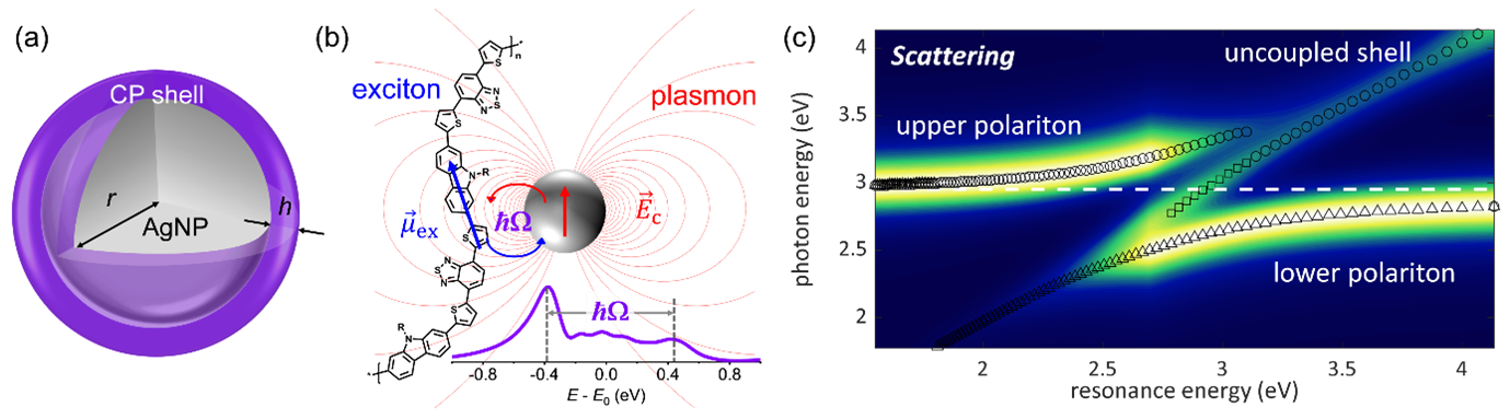
In this work, we explored plasmon-exciton coupling in Ag-conjugated polymer core-shell nanostructures (Figure 7a) using a combination of numerical finite-difference time-domain (FDTD) and analytical Mie theory calculations. Conjugated polymers have not been not been previously considered as candidates for strong coupling applications due to their broad spectral linewidths and multiple vibronic features. Here, we show that the linewidth of conjugated polymers plays a minimal role on the splitting energy between the plasmon-exciton-polariton modes (Figure 8a,b). We show that strong plasmon-exciton coupling can be achieved through the use of thick CP shells, large oscillator strengths (Figure 8c), modest high-frequency relative permittivities (Figure 8d), and multiple vibronic resonances (Figure 8e), all characteristic of typical conjugated polymers, and that Rabi splitting energies of over 1000 meV can be obtained using realistic material dispersive relative permittivity parameters.
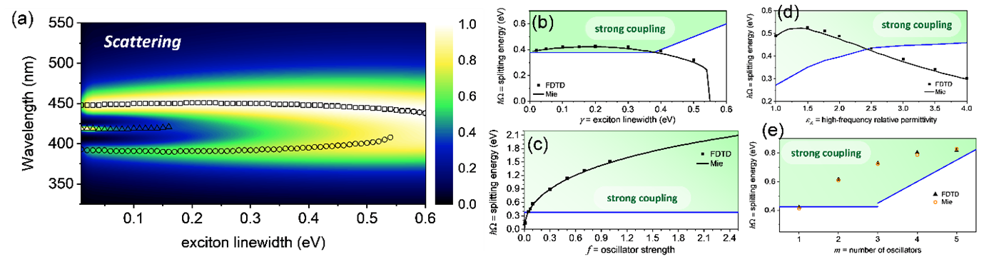
The results presented in this work give insight into the mechanisms of plasmon-exciton coupling when broadband excitonic materials featuring strong vibrational-electronic coupling are employed, and are relevant to organic optoelectronic devices and hybrid metal-organic photonic nanostructures.
References:
[1] F. Hide, et al. Semiconducting polymers: A new class of solid-state laser materials, Science 273, 1833-1836 (1996).
[2] J. D. Plumhof, et al. Room-temperature Bose-Einstein condensation of cavity exciton-polaritons in a polymer, Nature Materials 13, 247-252 (2014).
[3] P. Törmä and W. L. Barnes. Strong coupling between surface plasmon polaritons and emitters: A review, Rep. Prog. Phys. 78, 073901-013934 (2015).
4. Publications
4.1 Journals
- T. A. S. Doherty†, A. J. Winchester†, S. Macpherson, D. N. Johnstone, V. Pareek, E. M. Tennyson, S. Kosar, F. U. Kosasih, M. Anaya, M. Abdi-Jalebi, Z. Andaji-Garmaroudi, E. L. Wong, J. Madéo, Y.-H. Chiang, J.-S. Park, Y.-K. Jung, C. E. Petoukhoff, G. Divitini, M. K. L. Man, C. Ducati, A. Walsh, P. A. Midgley, K. M. Dani‡, and S. D. Stranks‡, Performance-limiting nanoscale trap clusters at grain junctions in halide perovskites, Nature 580, 360 (2020).
- M. Rumo, C. W. Nicholson, A. Pulkkinen, B. Hildebrand, G. Kremer, B. Salzmann, M.-L. Mottas, K. Y. Ma, E. L. Wong, M. K. L. Man, K. M. Dani, B. Barbiellini, M. Muntwiler, T. Jaouen, F. O. von Rohr, and C. Monney, Examining the surface phase diagram of IrTe2 with photoemission, Phys. Rev. B 101, 235120 (2020).
- D. R. Bacon, T. B. Gill, M. Rosamond, A. D. Burnett, A. Dunn, L. Li, E. H. Linfield, A. G. Davies, P. Dean, J. R. Freeman, Photoconductive arrays on insulating substrates for high-field terahertz generation, Optics Express 28 (12), 17219 (2020).
- C. E. Petoukhoff, K. M. Dani, and D. M. O'Carroll, Strong plasmon-exciton coupling in Ag nanoparticle - conjugated polymer core-shell hybrid nanostructures, Polymers, 12 (9), 2141 (2020).
- J. Madéo†, M. K. L. Man†, C. Sahoo, M. Campbell, V. Pareek, E L. Wong, A. Al-Mahboob, N. S. Chan, A. Karmakar, B. M. K. Mariserla, X. Li, T. F. Heinz, T. Cao, K. M. Dani, Directly visualizing the momentum-forbidden dark excitons and their dynamics in atomically thin semiconductors, Science 370 (6521), 1199 (2020).
†equal authors
Perspective: Meng Xing Na, Ziliang Ye, Probing the dark side of the exciton, Science 370 (6521), 1166 (2020).
Featured: C. Middleton, Photoelectrons shine a light on dark excitons, Phys. Today, 74, 16–18 (2021). - J. Pérez-Urquizo, Y. Todorov, L. Li, A. G. Davies, E. H. Linfield, C. Sirtori, J. Madéo, K. M. Dani, Monolithic patch-antenna THz lasers with extremely low beam divergence and polarization control, ACS Photonics 8(2), 412 (2021).
4.2 Books and other one-time publications
Nothing to report.
4.3 Oral and Poster Presentations
- Dani, K. M., The Quantum Psychology of Dark Excitons: The case of the traumatic separation, Seminar (online), Dept of Physics, Nanyang Technology University, Singapore, May 25th (2020).
- Winchester, A. J., Macpherson, S., Doherty, T., Petoukhoff, C. E., Dani, K. M., Visualizing Carrier Trapping at the Nanoscale in Hybrid Organic-Inorganic Perovskite Films, Oral Presentation (online), JSAP-OSA Joint Symposia, Osaka, Japan, Sep 8-11 (2020).
- Pareek, V., Madéo, J., Dani, K. M. Ultrafast control of the dimensionality of exciton-exciton annihilation in atomically thin black phosphorus, Oral Presentation (online), JSAP-OSA Joint Symposia, Osaka, Japan, Sep 8-11 (2020).
- Dani, K. M., Observing momentum-forbidden dark excitons in monolayer WSe2 via time-, space and angle-resolved photoemission spectroscopy, Invited Talk (online), NOEKS15, Muenster, Germany, Sep 13-17 (2020).
- Dani, K. M., Developing world-class nanophotonics research in India, Panel Discussion, Vaibhav Summit: Photonics Vertical, India, Oct 15th (2020)
- Man, M. K. L., Dani, K. M., Visualization of excitons in 2D semiconductors by time-resolved (µ)-ARPES, Invited Talk (online), Next Generation Spectro-Microscopy and Micro-Spectroscopy Workshop, Japan, Oct 28-29 (2020).
- Madéo, J., Man, M. K. L., Sahoo, C., Campbell, M., Pareek, V., Wong, E. L., Al-Mahboob, A., Chan, N.S., Karmakar, A., Mariserla, B. K. M., Li, X., Hsinz, T.F., Dani, K. M., Time-resolved ARPES of excitons in an atomically thinsemiconductor, Oral Presentation (online), Ultrafast Phenomena 2020, Shanghai, China, Nov 16-19 (2020).
- Pareek, V., Madéo, J., Dani, K. M., Controlling the Dimensionality of Exciton-Exciton Annihilation in Atomically Thin Black Phosphorus, Poster Presentation, Ultrafast Phenomena 2020, Shanghai, China, Nov 16-19 (2020).
- Dani, K. M., Imaging the distribution of the electron around the hole in an exciton, Seminar (online), Laboratoire Ondes et Matiere d’Aquitaine, University of Bordeaux, France, Jan 26th (2021).
- Dani, K. M., Into The Darkness: The Hunt for Forbidden Excitons, OIST Foundation U.S.-Japan Science Webinar, Feb 19th (2021).
- Dani, K. M., Imaging the ‘bond’ between the electron and hole in a photoexcited exciton, Colloquium, Physics Department, University of Alabama, U.S. Feb 26th (2021).
- Petoukhoff, C. E., Dani, K. M., O’Carroll, D. M., Strong Plasmon-Exciton Coupling in Ag-Conjugated Polymer Core-Shell Nanoparticles, Oral Presentation (online), APS March Meeting 2021, Boston, U.S. Mar 15-19 (2021).
- Dani, K. M., Probing the dark side of the exciton with time-resolved ARPES, Seminar (online), Center for Correlated Electron Systems, Institute for Basic Science, South Korea, Mar 12th (2021).
5. Intellectual Property Rights and Other Specific Achievements
Madéo, J., Man, M. K. L. and Dani, K. M. “Laser-driven microplasma XUV source,” US patent application 16/845,419, Oct 2020.
6. Meetings and Events
6.1 Seminar
- Date: February 10th 2021
- Venue: Online
- Speaker: Prof. Gil Refael
6.2 Workshop
Nothing to report.
7. Other
Nothing to report.