

FY2016 Annual Report
Femtosecond Spectroscopy Unit
Assistant Professor Keshav Dani
Abstract
In recent years, the ability to synthesize, engineer & observe materials on the nanometer length scale has led to novel phenomena and applications. On the other hand, modern lasers deliver powerful, ultrashort pulses of light allowing us to observe the interaction of electrons and atoms on the femtosecond timescale. Together, these technologies allow us to study new paradigms in light-matter interaction – with femtosecond temporal resolution and nanometer spatial resolution. In FY2016, Femtosecond Spectroscopy Unit has directed these abilities and made progress towards four different areas of study:
(a) Novel two-dimensional materials and their heterostructures, where we search for new functionality in materials with applications in optics, electronics and energy;
(b) Terahertz devices & applications, where we investigate the generation of broadband THz radiation and applying this to a variety of materials and devices;
(c) Femtosecond techniques for neuroscience & drug delivery, where femtosecond pulses and nanoscale, biocompatible devices offer new possibilities in imaging and interacting with the brain;
(d) Study of art conservation materials, where femtosecond pulses allow the cross-sectioning of delicate art materials with minimal damage.
1. Staff
- Dr. Keshav M. Dani, Professor
- Dr. Michael K. L. Man, Researcher
- Dr. Bala Murali Krishna, Researcher
- Dr. Takaaki Harada, Researcher
- Dr. Julien Madéo, Researcher
- Athanasios Margiolakis, Special Research Student
- Christopher Petoukhoff, Special Research Student
- E Laine Wong, Graduate Student
- Viktoras Lisicovas, Graduate Student
- Andrew Winchester, Graduate Student
- Vivek Pareek, Graduate Student
- Yumi Ito, Administrative Assistant
2. Collaborations
Theme: Novel two-dimensional materials and their heterostructures
- Type of collaboration: Joint research
- Researchers:
- Dr. Robert Vajtai, Ricer University, Houston, TX, USA
- Professor P.M. Ajayan, Rice University, Houston, TX, USA
- Prof. Z.-H. Loh, Nanyang Technology Univ. (NTU), Singapore
- Prof. M. Chhowalla, Rutgers University, NJ, USA
- Prof. D. M. O’Carroll, Rutgers Universty, NJ, USA
Theme: Terahertz Devices and Applications
- Type of collaboration: Joint research
- Researchers:
- Professor C. Sirtori, Universite Paris Diderot, Paris, France
- Dr. Y. Todorov, Universite Paris Diderot, Paris, France
- Prof. E. H. Linfield, University of Leeds, Leeds, UK
Theme: Femtosecond Techniques for Neuroscience and Drug Delivery
- Type of collaboration: Joint research
- Researchers:
- Professor J. Wickens, Okinawa Inst. Of Science and Tech., Japan
Theme: Study of Art Conservation Materials
- Type of collaboration: Joint research
- Researchers:
- Professor A. N. Shugar, Buffalo State University, NY, USA
- J. F. Hamm, Buffalo State University, NY, USA
- A. R. Dani, Okinawa Inst. Of Sci. & Tech., Okinawa, Japan
3. Activities and Findings
3.1 Novel Two-Dimensional Materials and Their Heterostructures
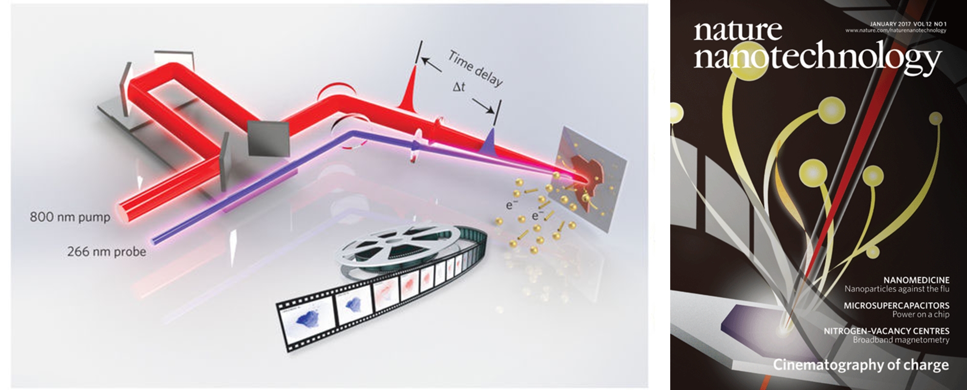
A. Imaging the motion of electrons across semiconductor heterojunctions
[Nature Nanotechnology 12, 36 (2017)]
Traditionally, carrier dynamics is studied with ultrafast optics in which time resolution of femtosecond or better is accomplished using very short laser pulses. However, due to the diffraction limit, optic technique has limited spatial resolution and it is insufficient to spatially resolve carrier dynamics in devices or nanostructures at the nanometer length scale. In the FSU, we overcome this resolution limit by imaging photoelectrons generated by the ultrafast laser pulse at high spatial resolution with a photoemission electron microscope. The unique combination of electron microscopy with ultrafast optics provide a means to visualize electron dynamics in materials at its fundamental time and length scale. Using this technique, for the first time, we captured a video showing electron flow and charge transfer within a photovoltaic device structure. This ultrafast nanoscale imaging technique provides a unique way to investigate novel materials and quantum processes in the nano- and femto- scale where the interaction of light and matter are still poorly understood.
References Section 3.1 A:
[1] M. K. L. Man, et al. Imaging the motion of electrons across semiconductor heterojunctions, Nat. Nanotech. 12, 36 (2017).
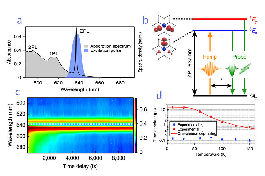
B. Jahn-Teller-induced femtosecond electronic depolarization dynamics of the nitrogen vacany defect in diamond
[Nature Communications 7, 13510 (2016)]
The negatively charged nitrogen-vacancy (NV -) defect has attracted the most attention, motivated by its potential to serve as a building block for novel quantum technologies. Single-photon emission from the nitrogen-vacancy defect in diamond constitutes one of its many proposed applications. Owing to its doubly degenerate 3E electronic excited state, photons from this defect can be emitted by two optical transitions with perpendicular polarization. Previous measurements have indicated that orbital-selective photoexcitation does not, however, yield photoluminescence with well-defined polarizations, thus hinting at orbital-averaging dynamics even at cryogenic temperatures. Here we employ femtosecond polarization anisotropy spectroscopy to investigate the ultrafast electronic dynamics of the 3E state (Fig. 2). We observe sub-picosecond electronic dephasing dynamics even at cryogenic temperatures, up to five orders of magnitude faster than dephasing rates suggested by previous frequency- and time-domain measurements. Ab initio molecular dynamics simulations assign the ultrafast depolarization dynamics to nonadiabatic transitions and phonon-induced electronic dephasing between the two components of the 3E state. Our results provide better understanding of the ultrafast orbital averaging that exists even at cryogenic temperatures.
References Section 3.1 B:
[1] R. Ulbricht, et al. Jahn-Teller-induced femtosecond electronic depolarization dynamics of the nitrogen-vacancy defect in diamond, Nat. Commun. 7, 13510 (2016).
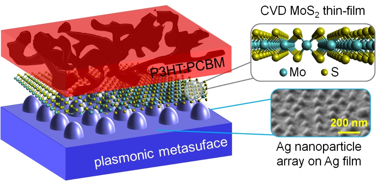
C. Ultrafast charge transfer and enhanced absorption in MoS2-Organic van der Waals heterojucntions using plasmonic metasurfaces
[ACS Nano 10, 9899 (2016)]
Since the isolation of graphene, there has been a tremendous interest in the exfoliation and subsequent stacking of van der Waals (vdW) materials – crystals that have strong in-plane covalent bonds in two-dimensional (2D) sheets but weak out-of-plane vdW bonding between sheets [1,2]. Monolayers of vdW materials lack dangling bonds, which enables the stacking of different layers to form vdW heterostructures without the rigorous requirements of traditional epitaxial growth methods. Recently, mixed-dimensional vdW heterojunctions, which are fabricated from 2D materials stacked with materials of different dimensionalities, have been of growing interest due to the possibility of assembling hybrid materials with novel functionalities [3]. Of particular interest are heterostructures between semiconducting transition metal dichalcogenides and organic semiconductors, which can serve as type-II photovoltaic heterojunctions due to the large absorption cross-sections of the individual materials [4-6]. However, although these novel organic-2D vdW heterojunctions have large absorption coefficients, their photovoltaic efficiency is still very low – less than 1% -due to restrictions on the physical thickness of both materials.
In this work, we employed plasmonic metasurfaces to enhance the absorption and charge photogeneration within a physically thin organic-2D vdW heterojunction (Figure 3). Plasmonic nanostructures and metasurfaces have been shown to increase absorption in ultrathin films and 2D semiconductors, and thus are good candidates for improving absorption in vdW heterojunctions [7-9]. We investigated the ultrafast charge transfer dynamics between an organic polymer:fullerene blend and large-area chemical vapor deposition (CVD)-grown monolayer MoS2 using transient pump-probe reflectometry. With the plasmonic metasurface, the charge photogeneration within the polymer was enhanced 6-fold, and the total active layer absorption bandwidth was increased by 90 nm relative to the polymer:fullerene blend alone. In the FSU, we demonstrated, for the first time, that photoinduced charge transfer from MoS2 to an organic semiconducting polymer occurs at ultrafast (< 100 fs) time scales, and that this charge transfer facilitates the significant enhancement in charge carrier density within the organic semiconducting polymer in the presence of the plasmonic metasurface.
References Section 3.1 C:
[1] A. K. Geim and I. V. Grigorieva Van der Waals Heterostructures, Nature 499, 419 (2013).
[2] Liu, Y., et al. Van der Waals Heterostructures and Devices, Nature Reviews Materials 1, 16042 (2016).
[3] Jariwala, D., et al. Mixed-Dimensional van der Waals Heterostructures, Nature Materials 16, 170 (2017).
[4] Homan, S. B., et al. Ultrafast Exciton Dissociation and Long-Lived Charge Separation in a Photovoltaic Pentacene-MoS2 van der Waals Heterojunction, Nano Lett. 17, 164 (2017).
[5] Liu, F., et al. Van der Waals p-n Junction Based on an Organic-Inorganic Heterostructure, Adv. Funct. Mater. 25, 5865 (2015).
[6] Shastry, T. A., et al. Mutual Photoluminescence Quenching and Photovoltaic Effect in Large-Area Single-Layer MoS2-Polymer Heterojunctions, ACS Nano 10, 10573 (2016).
[7] Petoukhoff, C. E., et al. Plasmonic Electrodes for Bulk-Heterojunction Organic Photovoltaics: A Review, J. Photon. Energy 5, 057002 (2015).
[8] Pandey, A. K., et al. Nanostructured, Active Organic-Metal Junctions for Highly Efficient Charge Generation and Extraction in Polymer-Fullerene Solar Cells, Adv. Mater. 24, 1055 (2012).
[9] Jariwala, D., et al. Near-Unity Absorption in van der Waals Semiconductors for Ultrathin Optoelectronics, Nano Lett. 16, 5482 (2016).
3.2 Terahertz Devices and Applications
A. Patch antenna microcavity terahertz sources with enhanced emission
[Applied Physics Letters 109, 141103 (2016)]
Realizing efficient sources and detectors at terahertz (THz) frequencies is of importance as this opens the way to a wide range of potential applications such as molecular spectroscopy, imaging, security scanning and investigation of low energy physical and chemical interactions [1]. In previous fiscal years, the unit has demonstrated semiconductor-based THz sources based on ultrafast laser excitation for spectroscopic applications [2,3]. In FY2016, we have investigated electrically injected THz sources based on quantum cascade (QC) active regions [4] and studied the enhancement of THz electroluminescence in the microcavity regime. In particular, we have investigated THz emission from arrays of antenna-coupled microcavities also called patch antenna microcavities and explored the effect of strong subwavelength electromagnetic confinement combined with the array geometry [5].
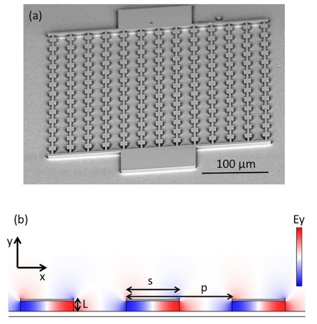
Patch antenna microcavities are metal-semiconductor-metal subwavelength resonators structures in square shapes. The length s of the resonator defines the resonant frequency of the resonator via s=l/2n, with the refractive index of the mode. In addition, these microcavities are vertical emitters as they emit as patch antennas. We have studied the emission of samples by varying the distance d between resonators composing the array, the active region thickness (4.5 THz QC active region) and the length s of the resonators (Fig. 4). At fixed period of the array, a clear enhancement was observed for s=11 µm, corresponding to the resonator resonant frequency being in resonance with the QC electronic radiative transition, a signature of Purcell effect. By measuring the emission with d ranging from 5 to 40 µm and L=2 and 4 µm, we observed up to 44-fold enhancement of spontaneous emission compared to a reference sample consisting of a large etched mesa (Fig.5).
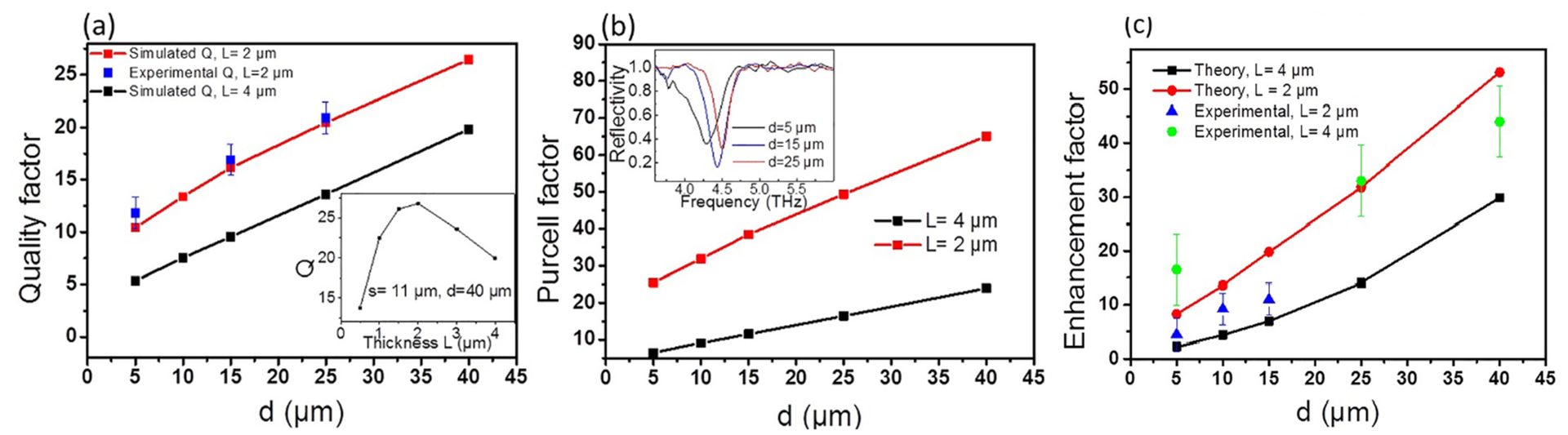
By comparing our experimental with finite element simulations and antenna theory, we extract record Purcell factors in the THz range of 65 and high photon out-coupling efficiencies larger than 60%. Furthermore, our results show that the quality factor of the array increases linearly with the distance d between resonators directly impacting the Purcell factor and photon out-coupling. Our work opens the way to achieve efficient surface emitting THz quantum cascade lasers and devices based on optical nonlinearities such intracavity difference frequency or second harmonic generation.
References Section 3.2 A:
[1] M. Tonouchi, Cutting-edge terahertz technology, Nat. Photonics 1, 97-105 (2007).
[2] P. J. Hale, et al. 20 THz broadband generation using semi-insulating GaAs interdigitated photoconductive antennas, Optics Express 22, 26358 (2014).
[3] J. Madéo, et al. Ultrafast properties of femtosecond-laser-ablated GaAs and its application to terahertz optoelectronics, Optics Lett. 40, 3388-3391 (2015).
[4] R. Kohler, et al. Terahertz semiconductor-heterostucture laser, Nature 4, 156-159 (2002).
[5] J. Madéo, et al. Patch antenna microcavity terahertz sources with enhanced emission, Appl. Phys. Lett. 109, 141103 (2016).
3.3 Femtosecond Techniques for Neuroscience and Drug-Delivery
A. Interfacing with neural activity via femtosecond laser stimulation of drug encapsulating liposomal nanostructures
[eNeuro 3, e0107 (2016)]
During FY16, the Femtosecond Spectroscopy Unit has continued their work with the Wickens Unit at OIST to explore the use of femtosecond pulses in stimulating and interacting with neurons via the on-demand release of neurochemicals from liposomes. Previous experiments [Ref] demonstrated the ability to release dopamine and other chemicals on demand from liposomes packed with the chemical by stimulating with a femtosecond laser pulse train.
In FY16, this work was extended to demonstrating the release of a wide range of chemicals, including inhibitory and excitatory neurochemicals, as well as synthetic analogs of naturally occurring chemicals. Furthermore, these releases were shown to evoke sub and supra changes in membrane potential in live brain slices, bringing the technique closer to in vivo studies in mice, and corresponding applications. We showed that the responses were repeatable and could be controlled by adjusting laser stimulation characteristics. In particular, we demonstrated the release of a synthetic receptor-specific agonist that exerts physiological effects on long-term synaptic plasticity. Lastly, we also demonstrated that the loaded liposomal nanostructures can remain functional in a live mouse for long periods – upto several days or weeks.
3.4 Study of Art Materials
A. Obtaining cross-sections of paint layers in cultural artifacts using femtosecond pulsed lasers
[Materials 10, 107 (2017)]
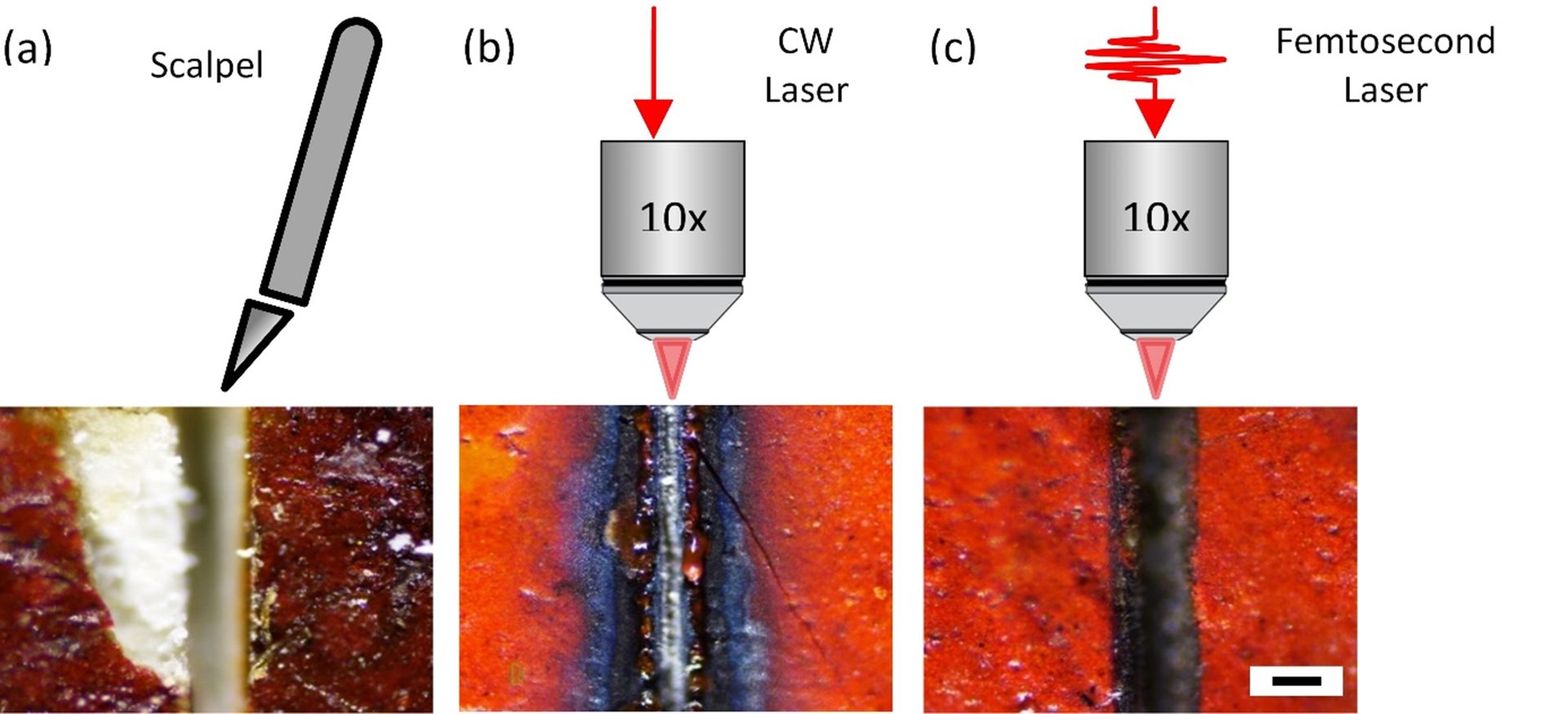
Over the past decade, it has been shown that ultrafast lasers provide the ability to machine metals and dielectrics with high precision and minimal thermal damage, due to their high peak powers and short pulse durations. In FY16, using this broad concept of machining with femtosecond lasers, the Femtosecond Spectroscopy Unit, in collaboration with the Art Conservation Program at OIST, and the Art Conservation Department at Buffalo State University studied a novel application to art materials - obtaining cross-sections of fragile, combustible paint layers in artwork and cultural heritage property. In general, cross-sections of paint and other decorative layers on artwork are essential to study art work and obtain useful information including fundamental knowledge about the materials used, the stratigraphy of the original and restored layers, and the history and authenticity of the art. However, current techniques to obtain cross-sections use scalpels, which can cause further damage to the artwork during the process of obtaining the cross-section, (such as crumbling, delamination, and paint compression), due to the pressure applied during a scalpel cut. Laser cutting offers an interesting alternative where one would not have to apply additional pressure while obtaining a cross-section. However, typical lasers, such as continuous-wave (CW) or nanosecond pulsed lasers can cause oxidative damage to combustible artwork.
In this collaboration, we demonstrated that femtosecond pulsed lasers allow one to make controlled cross-sections of paint layers, with minimal to no damage to the surrounding artwork. The femtosecond laser cutting can avoid problems such as fragile paint disintegrating under scalpel pressure, or oxidation by the CW laser. By varying the laser power and translational speed of the laser over the art work during the cutting process, we noted different benefits for cross-section sampling. In general, our work on the use of femtosecond lasers in studying artwork presents new possibilities in analyzing, sampling, and cleaning of artwork with minimal destructive effects.
References Section 3.4 A:
[1] T. Harada, et al. Obtaining cross-sections of paint layers in cultural artifacts using femtosecond pulsed lasers, Materials 10, 107 (2017).
4. Publications
4.1 Journals
- Takaaki Harada†, Stephanie Spence†, Athanasios Margiolakis, Skylar Deckoff-Jones, Rebecca Ploeger, Aaron N. Shugar, James F. Hamm, Keshav M. Dani and Anya R. Dani, Obtaining cross-sections of paint layers in cultural artifacts using femtosecond pulsed lasers, Materials 10, 107 (2017). †These authors contributed equally to this work.
- M. K. L. Man, A. Margiolakis, S. Deckoff-Jones, T. Harada, E L. Wong, M. B. M. Krishna, J. Madéo, A. Winchester, S. Lei, R. Vajtai, P. M. Ajayan and K. M. Dani, Imaging the motion of electrons across semiconductor heterojunctions, Nat. Nanotechnol. 12, 36 (2017).
- R. Ulbricht, S. Dong, I-Y. Chang, B. M. K. Mariserla, K. M. Dani, K. Hyeon-Deuk, and Z.-H. Loh. Jahn-Teller-induced femtosecond electronic depolarization dynamics of the nitrogen-vacancy defect in diamond, Nat. Commun. 7, 13510 (2016).
- C. E. Petoukhoff, M. B. M. Krishna, D. Voiry, I. Bozkurt, S. Deckoff-Jones, M. Chhowalla, D. M. O'Carroll, and K. M. Dani. Ultrafast charge transfer and enhanced absorption in MoS2 - organic van der Waals heterojunctions using plasmonic metasurfaces, ACS Nano 10, 9899 (2016).
- T. Nakano, S. M. Mackay, E. W. Tan, K. M. Dani, and J. Wickens. Interfacing with neural activity via femtosecond laser stimulation of drug encapsulating liposomal nanostructures, eNeuro 3, e0107 (2016).
- J. Madéo, Y. Todorov, A. Gilman, G. Frucci, L. H. Li, A. G. Davies, E. H. Linfield, C. Sirtori and K. M. Dani, Patch antenna microcavity terahertz sources with enhanced emission, Appl. Phys. Lett. 109, 141103 (2016).
4.2 Books and Other One-Time Publications
Nothing to report.
4.3 Oral and Poster Presentations
- Dani, K. M., Man, M. K. L., Deckoff-Jones, S., Harada, T., Wong, E., Margiolakis, A., Mariserla, B. M. K., Madeo, J., Winchester, A., Lei, S., Vajtai, R., Ajayan, P. M. Time Resolved Photoemission Electron Microscopy of Nanoscale Semiconductor Heterojunctions, Invited Talk, TERAMETANANO-2016, Cartagena, Colombia, Apr 03-10 (2016).
- Dani, K. M., Ultrafast electron dynamics in 2D van der Waals crystals, Invited Talk, RD2DS-2016: Recent Development in 2D Systems, Okinawa Institute of Science and Technology Graduate University Okinawa, Japan, Apr 04-08 (2016)
- Berggren, B. S., Harada, T., Deckoff-Jones, S., Renaud, D., Winchester, A., Madeo, J., Hu, J., Liu, X., Mao, Z., Wei, J., Talbayev, D., Weber, C., Dani, K. M. Transient Reflectivity Measurements Reveal Photo-Carrier Dynamics in Two-Dimensional Black Phosphorus, Poster Presentation, RD2DS-2016: Recent Development in 2D Systems, Okinawa Institute of Science and Technology Graduate University Okinawa, Japan, Apr 04-08 (2016)
- Harada, T., Berggren, B. S., Deckoff-Jones, S., Renaud, D., Winchester, A., Madeo, J., Hu, J., Liu, X., Mao, Z., Wei, J., Talbayev, D., Weber, C., Dani, K. M. Stabilization of Black Phosphorus by Hexagonal-Boron Nitride and Thin Chromium film, Poster Presentation, RD2DS-2016: Recent Development in 2D Systems, Okinawa Institute of Science and Technology Graduate University Okinawa, Japan, Apr 04-08 (2016)
- Madeo, J., Deckoff-Jones, S., Zhang, J., Petoukhoff, C., Man, M. K. L., Lei, S., Vajtai, R., Ajayan, P. M., Talbayev, D., Dani, K. M. Observing the interplay between surface and bulk optical nonlinearities in thin van der Waals crystals, Oral Presentation, CLEO2016, San Jose, CA USA Jun 05-10 (2016).
- Harada, T., Berggren, B. S., Deckoff-Jones, S., Renaud, D., Winchester, A., Madeo, J., Hu, J., Liu, X., Mao, Z., Wei, J., Talbayev, D., Weber, C., Dani, K. M. Nonlinear Optical Responses of Protected Atomically Thin Black Phosphorus, Oral Presentation, CLEO2016, San Jose, CA, USA Jun 05-10 (2016).
- Madeo, J., Todorov, Y., Gilman, A., Frucci, G., Li, L., Linfield, E., Sirtori, C., Dani, K. M. Patch antenna microcavities terahertz sources with enhanced emission, Oral Presentation, CLEO2016, San Jose, CA, USA Jun 05-10 (2016).
- Man, M. K. L. Ultrafast and Nonlinear Dynamics in 2D Materials and their heterostructures, Oral Presentation, CIMTEC 2016, Perugia, Italy, Jun 05-09 (2016).
- Man, M. K. L., Deckoff-Jones, S., Harada, T., Wong, E., Margiolakis, A., Mariserla, B. M. K., Madeo, J. Imaging the flow of electrons in 2D semiconductor heterojunctions, Oral Presentation, Graphene Week 2016, Warszawa, Poland, Jun 13-17 (2016)
- Dani, K. M., Man, M. K. L., Margiolakis, A., Deckoff-Jones, S., Harada, T., Wong, E., Mariserla, B. M. K., Madeo, J., Winchester, A., Lei, S., Vajtai, R., Ajayan, P. M. Into the rabbit hole - tracking electrons through energy momentum, space and time, Invited Talk, UDN 2016, Okinawa Institute of Science and Technology Graduate University Okinawa, Japan, July 13-16 (2016)
- Petoukhoff, C. E., Mariserla, B. M. K., Voiry, D., Bozkurt, I., Deckoff-Jones, S., Chhowalla, M., O’Carroll, M., Dani, M. K. Ultrafast Charge Transfer in MoS2 – Organic van der Waals Heterojunctions using Plasmonic Matasurfaces, Poster Presentation, UDN 2016, Okinawa Institute of Science and Technology Graduate University Okinawa, Japan, July 13-16 (2016)
- Wong, E., Winchester, A., Man, M. K. L., Pareek, V., Madeo, J., Dani, K. M. Flipping the flow of charge with light in a PN junction, Poster Presentation, UDN 2016, Okinawa Institute of Science and Technology Graduate University Okinawa, Japan, July 13-16 (2016)
- Lisicovas, V., Harding, R., Maruyama, I., Dani, K. M. Imaging the Formation of Memories in C. Elegans using a Wide-Field Temporally Focused Two-Photon Microscope, Poster Presentation, UDN 2016, Okinawa Institute of Science and Technology Graduate University Okinawa, Japan, July 13-16 (2016)
- Bryan, B., Harada, T., Weber, C., Renaud, D., Winchester, A., Deckoff-Jones, S., Hu, J., Liu, X., Mao, Z., Wei, J., Talbayev, D., Mariserla, B. M. K., Madeo, J., Dani, M. K. Ultrafast Properties of Atomically Thin Black Phosphorus, Poster Presentation, UDN 2016, Okinawa Institute of Science and Technology Graduate University Okinawa, Japan, July 13-16 (2016)
- Man, M. K. L. Margiolakis, A., Deckoff-Jones, S., Harada, T., Mariserla, B. M. K., Wong, E., Madeo, J., Winchester, A., Lei, S., Vajtai, R., Ajayan, P. M., Dani, K. M. Visualization of Electron in motion in 2D Semiconductor Heterojunctions, Oral Presentation, Ultrafast Phenomena 2016, Santa Fe, NM, USA, Jul 17-22 (2016)
- Mariserla, B. M. K., Madeo, J., Margiolakis, A., Zhao, Z-Y., Hale J., Man, M. K. L., Zhao, Q. Z., Peng, W., Shi, W. Z., Dani, K. M. Optoelectronic Properties in the Terahertz of Femtosecond-laser-ablated GaAs, Invited Talk, PIERS, Shanghai, China, Aug 08-11 (2016)
- Man, M. K. L., Margiolakis, A., Deckoff-Jones, S., Harada, T., Mariserla, B. M. K., Wong, E., Madeo, J., Winchester, A., Lei, S., Vajtai, R., Ajayan, P. M., Dani, K. M. Visualization of Electron in motion in 2D Semiconductor Heterojunctions, Oral Presentation, LEEMPEEM-10, Monterey, CA, USA, Sep 11-15 (2016)
- Man, M. K. L., Winchester, A., Yamaguchi, H., Gupta, G., Mohite, A. D., Najmaei, S., Lei, S., Talapatra, S., Ajayan, P. M., Lou, J., Dani, K. M. Structural order and substrate mediated corrugation in CVD grown molybdenum disulphide, Poster Presentation, LEEMPEEM-10, Monterey, CA, USA, Sep 11-15 (2016)
- Winchester, A., Man, M. K. L., Deck-off Jones, S., Harada, T., Wong, E., Margiolakis, A., Mariserla, B. M. K., Madeo, J., Lei, S., Vajtai, R., Ajayan, P. M., Dani, K. M., Visualizing electrons flow in 2D semiconductor heterojunctions, Poster Presentation, LEEMPEEM-10, Monterey, CA, USA, Sep 11-15 (2016)
- Wong, E., Winchester, A., Man, M. K. L., Pareek, V., Madeo, J., Dani, K. M., Probing charge carrier dynamics in doped GaAs using time-resolved photomission spectroscopy, Poster Presentation, LEEMPEEM-10, Monterey, CA, USA, Sep 11-15 (2016)
- Dani, K. M, Harada T., Spence, S., Margiolakis, A., Deckoff-Jones, S., Shugar, A., Hamm, J., Dani, A. R. Creating Cross-Sections of Fragile Paint Layers in Artwork using Femtosecond Lasers, Invited Talk, Workshop on Advanced Analytical Imaging Methods in the Conservation of Works of Art, Tokyo Japan, Nov 28 (2016)
- Mariserla, B. M. K., Madeo, J., Vinod, S., Tiwary, C. S., Ajayan, P. M., Dani, K. M. THz transient dynamics and photoconductivity in liquid exfoliated van der Waals insulator-semiconductor heterostructure laminates, Oral Presentation, Photonics 2016, IIT Kanpur, India, Dec 04- 08 (2016)
- Petoukhoff, C. E., Mariserla, B. M., K., Dani, K. M., O’Carroll, D. M. Strong Coupling between Surface Plasmons and Excitons in Conjugated Polymers, Oral Presentation, 2016 Materials Research Society Fall Meeting, Boston, MA, USA, Nov 27- Dec 02 (2016)
- Dani, K. M. Time-resolved photoemission of semiconductor heterostructures, Invited Talk, SPIE Photonics West OPTO 2017, San Francisco, CA, USA, Jan 28-Feb 02 (2017)
- Man, M. K. L. Imaging electrons motion in semiconductor materials, Invited Talk, 7th Annual Congress on Materials Research and Technology, Berlin, Germany, Feb 20-21 (2017)
- Pareek, V., Madeo, J., Dani, K. M. Generating fourth harmonic of 800 nm femtosecond laser, Poster Presentation, The Science Challenge, Okinawa Institute of Science and Technology Graduate University Okinawa, Japan, Mar 06-10 (2017)
- Dani, K. M. Imaging the motion of electrons in 2D semiconductor heterostructures, Invited Talk, March Meeting American Physical Society, New Orleans, LA, USA, Mar 13-17 (2017)
5. Intellectual Property Rights and Other Specific Achievements
Nothing to report.
6. Meetings and Events
6.1 Seminar
- Date: Nov 2nd 2016
- Venue: OIST Campus Center Buld
- Speaker: Dr. Said Rahimzadeh-Kalaleh Rodriguez
- Date: Nov 7th 2016
- Venue: OIST Campus Center Buld
- Speaker: Prof. Yann Gallais
- Date: Feb 9th 2017
- Venue: OIST Campus Center Buld
- Speaker: Prof. Kung-Hsuan Lin
6.2 Workshop
Ultrafast Dynamics at the Nanoscale 2016 (UDN 2016)
- Date: June 30- July 4 (2015)
- Date: July 13-16, 2016
- Venue: OIST Campus Lab1
- Co-organizer:
- Prof. Hrvoje Petek (Univ. of Pittsburgh, USA)
- Prof. Junichiro Kono (Rice University, USA)
- Speakers:
- Dr. Tony Heinz (Stanford Univ., USA)
- Dr. Rupert Huber (Univ. of Regensburg, Germany)
- Dr. Junichiro Kono (Rice Univ., USA)
- Dr. Ursula Keller (ETH Zurich, Switzerland)
- Dr. Kuniaki Konishi (Tokyo Univ., Japan)
- Dr. Alfred Leitenstorfer (Univ. of Konstanz, Germany)
- Dr. Xiaoqin Li (Univ. of Texas- Austin, USA)
- Dr. Kaihui Liu (Peking Univ., China)
- Dr. Eric Potma (Univ. of California- Irvine, USA)
- Dr. Ron Shen (Univ. of California at Berkeley, USA/ Fudan Univ., China)
- Dr. Christopher Stanton (Univ. of Florida, USA)
- Dr. Antoniette Taylor (Los Alamos National Lab, USA)
- Dr. Yoshihisa Yamamoto (Cabinet Office, Govt. of Japan/ Stanford Univ. USA)
- Dr. Ulrike Woggon (Technische Universitat Berlin, Germany)
- Dr. Martin Wolf (Fritz Haber Institution, Germany)
7. Others
Nothing to report.