

FY2012 Annual Report
Femtosecond Spectroscopy Unit
Assistant Professor Keshav Dani
Abstract
Over the past few decades, techniques in ultrafast spectroscopy have opened the doors to study processes in materials with femtosecond (~10-15 second) temporal resolution, as well as study light matter interactions in the extremely nonlinear regime (~109 J/s). With these techniques, one can investigate, for example, chemical reactions unfold within picoseconds and make highly nonlinear optical devices for applications in telecommunications. In the Femtosecond Spectroscopy Unit, we use these techniques of ultrafast spectroscopy towards developing new instrumentation, and towards applications in Condensed Matter Physics, Surface Science, Materials Science and Biology. Below we present a brief report of the advances made and techniques developed by the Femtosecond Spectroscopy Unit in each of these topics.
1. Staff
- Dr. Keshav M. Dani, Professor
- Dr. Julien Madeo, Researcher
- Dr. Eleftheria Kavousanaki, Researcher
- Dr. Peter Hale, Researcher
- Dr. Michael Man, Researcher
- Catherine Chin, Graduate Student
- Rakesh Parayil, Graduate Student
- Atish Agarwala, Undergraduate Student
- Dr. Grigoris Panotopoulos, Guest Researcher
- Ms. Yoko Fujitomi, Research Administrator
2. Collaborations
- Theme: Ultrabroadband THz Spectroscopy with Interdigitated Antennas
- Type of collaboration: Joint research
- Researchers:
- Prof. Jerome Tignon, Ecole Normale Superieure, Paris, France
- Dr. Sukhdeep Dhillon, Ecole Normale Superieure, Paris, France
- Dr. Juliette Mangeney, Ecole Normale Superieure, Paris, France
- Matthieue Baillergeau, Ecole Normale Superieure, Paris, France
- Theme: Transient Photoconductivity Dynamics in Nitrogen Doped TiO2 for Photocatalytic Applications
- Type of collaboration: Joint research
- Researchers:
- Prof. Ivan Parkin, University College London, London, UK
- Alison J. Cross, University College London, UK
- Theme: Drug Delivery using Femtosecond Pulses
- Type of collaboration: Joint research
- Researchers:
- Prof. Jeff Wickens, OIST, Okinawa, Japan
- Dr. Takashi Nakano, OIST, Okinawa, Japan
3. Activities and Findings
3.1 NOVEL INSTRUMENTATION:
Terahertz radiation (1012 Hz) covers an important part of the electromagnetic spectrum between high speed electronnics (1 GHz) and below far-infrared optical radiation (1014 Hz). This region of the spectrum has important applications in pharmaceuticals through vibrational spectroscopy of molecules, biomedical applications through imaging of cancer cells and living tissues, and security industry through non-destructive, see-through imaging of concealed objects. However, the lack of good sources and detectors in this region of the spectrum has hindered large scale applications.
Typical sources of THz radiation today use complicated nonlinear optics with high power lasers, or small antenna structures where laser alignment is complex. Here, we have pushed the limits on a novel type of antenna structure (Intedigitated Antennas) in combination with short ultrafast pulses (~15 fs) to generate broadband terahertz (THz) radiation. The THz optical system was constructed in FY2011 with a demonstration that a bandwidth of up to 10 THz was measurable.
In FY2012, we have pushed the limits of this technology significantly to now generate beyond 25 THz. We have utilized large area interdigitated photoconductive antennas (Figure 1, inset) for high E-field THz generation, and a high repetition rate, high power oscillator laser. THz E-field calculations show that we are generating towards (and possibly beyond) 1 kV/cm of broadband THz radiation. The large bandwidth has been confirmed using a standard absorption sample, a thin PTFE tape to show a clear resonance at 15 THz, Figure 2.
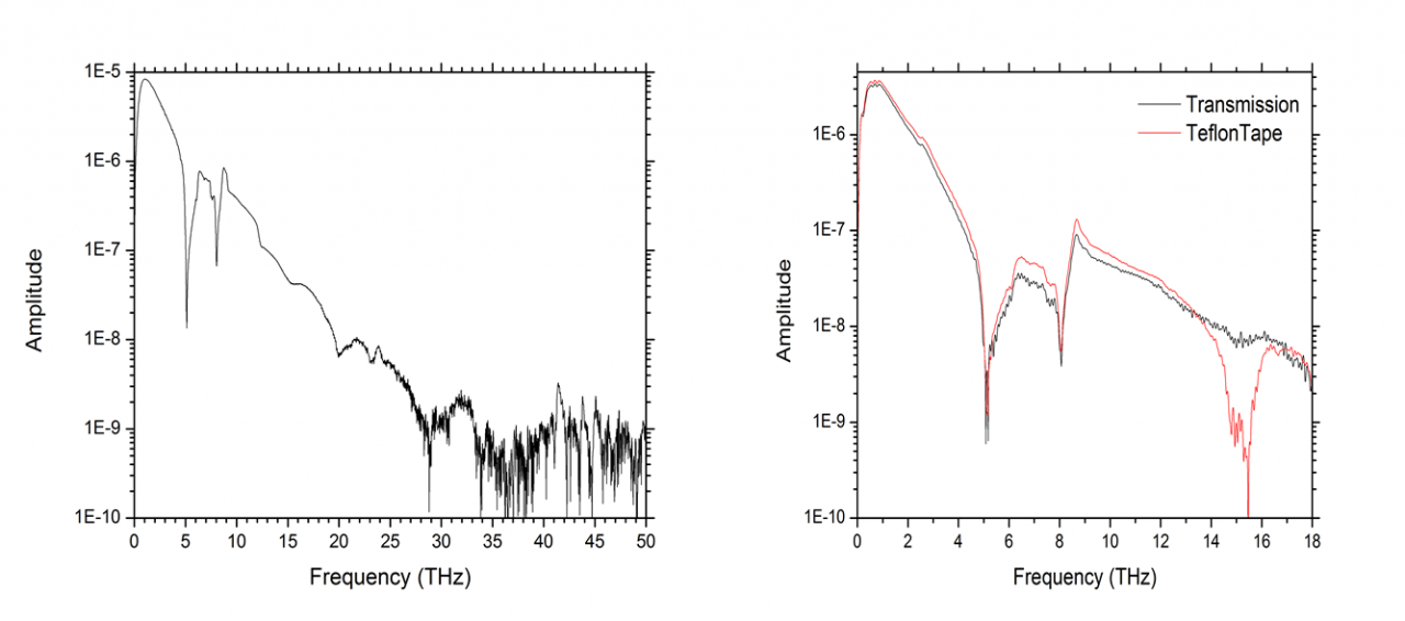
Figure 1: (Left) Spectrum of the Ultrabroadband THz Pulse showing a capability beyond 25 THz. (Right) A measurement of the absorption peaks in Teflon at ~15 THz to demonstrate the spectroscopic capability of the system.
3.2 CONDENSED MATTER PHYSICS
Optical selection rules in triangular graphene quantum dots [E. G. Kavousanaki, K. M. Dani]
Graphene quantum dots have attracted a lot of attention lately due to their unusual energy spectrum that depends strongly on the quantum dot size, shape and edge topology. It has been shown theoretically [1-2] that triangular quantum dots with zigzag type of edges exhibit a number of highly degenerate zero-energy states that are half filled at low temperatures and lead to a non-zero ground state magnetic moment (Figure 2a). In contrast, quantum dots with armchair type of edges exhibit a well-defined band gap and a semiconductor-like behavior. Experimentally though this behavior is still to be observed, partly because of the difficulties in controlling the shape and type of edges during manufacturing. Our work aims at understanding the optical properties of these structures and possibly suggesting ways of optically identifying the presence of these zero-energy states in a distribution of quantum dots of different edges and sizes.
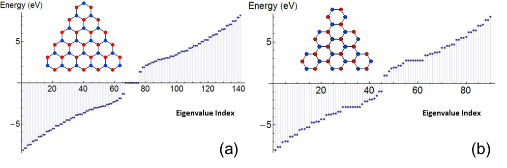
Figure 2: Energy spectrum for a triangular quantum dot with N = 10 atoms per side and (a) zigzag, and (b) armchair edges.
For our calculations we used the standard tight-binding model for graphene [3] to study its energy spectrum and eigenstates for different quantum dot sizes and edges and we calculated the oscillator strength for all possible transitions. Because of the triangular symmetry, we classified all eigenstates into three groups depending on their symmetry under a 120 degree rotation. We found that for circularly polarized light only transitions between states of specific symmetry are allowed.
These selection rules simplify the optical interactions of this important system, and provide a playground for manipulating the spin states and Fermi level states of this important nanoscale system.
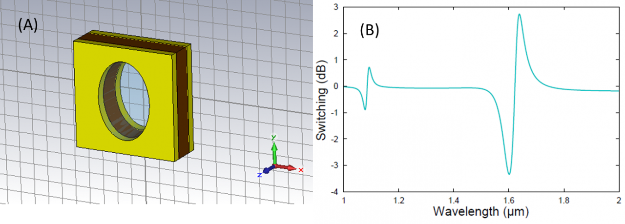
Geometric optimization of energy consumption in a metamaterial device for telecommunication [Atish Agarwala, K. M. Dani]
3.3 MATERIALS SCIENCE
Transient photoconductivity dynamics in Nitrogen doped TiO2 for Photocatalytic Applications [Catherine Chin, K. M. Dani]
Semiconductor photocatalysis, particularly using visible light, offers promising applications such as fuel production via hydrogen generation, and water and air purification [1]. However, most of the common photocatalysts, such as titanium dioxide (TiO2), make inefficient use of the solar spectrum due to large optical bandgaps in the UV. Recently, efforts have been directed towards increasing the visible light absorption of photocatalysts like TiO2 via doping [2]. However, typically this increased visible light absorption results in decreased reactivity, potentially due to dopant-induced scattering events that reduce photocarrier conductivity, mobility and lifetime. Optical Pump/THz Probe Spectroscopy is ideally suited to study the sub-picosecond dynamics of photoexcited carriers and their transient conductivity.
In this project, we photoexcite Nitrogen doped TiO2 (N-TiO2) films with ultrafast pulses in the UV and Visible, and then probe the photoexcited samples with sub-picosecond THz pulses to study the transient photoconductivity of the carriers. We observe clear differences in the picosecond dynamics of the photogenerated carriers as we vary nitrogen concentration and excitation wavelength. These differences are expected to directly impact the photocatalytic ability, and thus provide insight into engineering the efficiencies of these films for future applications.
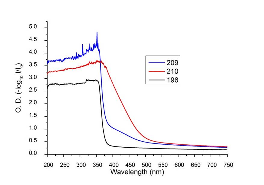
Figure 4: Absorption Spectrum of the three samples (Undoped - 196, Doped 209 & 210) showing increased absorption in the visible due to different types of nitrogen doping.
In collaboration with the Parkin Group at Univ. College London, we have grown samples of TiO2 films on quartz substrates by CVD with varying amounts of nitrogen doping. With UV-Vis absorption measurements we confirm increased absorption in the visible due to nitrogen doping (Figure 4). We excite our samples with ~ 100 fs pulses of 480 nm (absorption onset for doped samples) to 330 nm (above bandgap excitation), and then probe with a time-delayed THz pulse. We observe this despite the increased visible absorption, the N-TiO2 samples demonstrate decreased carrier mobility and faster relaxation rates, which directly impact their photocatalytic ability.
In conclusion, UV-Vis Pump/THz probe provides a new tool to directly access the ultrafast, microscopic dynamics of charge carriers in visible light photocatalysts, like N-TiO2 films. These results provide fundamental insight into the future engineering of these materials for more efficient use of the solar spectrum for a variety of applications.
3.4 BIOLOGY & MEDICINE
Drug Delivery Using Femtosecond Pulses [Peter Hale, Catherine Chin, K. M. Dani]
Recently developments in materials and nanotechnology have allowed for the development of biocompatible materials that can be introduced into the body and externally controlled via physical, chemical or biological stimulus. The high power of femtosecond pulses in particular allows for specific control of biomaterials by using their nonlinear optical properties.
In FY2012, the Femtosecond Spectroscopy Unit, in collaboration with the Wickens Unit at OIST has been developing a novel technique for controlling biocompatible drug delivery systems using femtosecond pulses.
3.5 SURFACE SCIENCE
Development of Low Energy Electron Microscopy with Femtosecond Spectroscopy [Michael Man, K. M. Dani]
Low energy electron microscopy and photoemission electron microscopy (LEEM/PEEM) is a powerful and versatile technique capable of performing surface characterization at spatial resolution down to the nanometer range. With LEEM/PEEM, one can image and perform spatially resolved structural, chemical and magnetic characterization of surface nanostructures.
One goal of the Femtosecond Spectroscopy Unit is to combine the time resolution of ultrafast spectroscopy technique with the spatial resolution of LEEM/PEEM microscopy. The photo-emitted electrons generated by the femtosecond laser will provide time resolution at ultrafast timescale, when combined with the LEEM/PEEM, it enables visualization of ultrafast dynamic processes, such as charge carrier dynamics during photexcitation and spin dynamics in magnetic nanomaterials, at the femtosecond temporal resolution and at nanometer spatial resolution. The possibly of imaging ultrafast dynamics in nanomaterials advances our understanding of the fundamental working principles behind the emerging nanotechnologies.
In February 2013 (the end of FY2012), the installation and testing of the LEEM/PEEM system was completed. The LEEM/PEEM system is in the process of being coupled to the femtosecond laser system and this will be done in the coming fiscal years. In the meantime, in FY2012, efforts were directed towards the initial preparation of samples, in particular, of 2D materials like Graphene, hexagonal-Boron Nitride and Molybdenum Disulfide in the LEEM/PEEM.
By the end of March 2013 (end of FY2012), we have also setup an inert atmosphere glovebox system in our laboratory. The glovebox system enables transfer and exchange of environmental sensitive test material among different units and collaborators. It facilitates investigation of advanced materials which cannot be prepared in the LEEM/PEEM system.
4. Publications
4.1 Journals
- Dani, K. M., Sharma , J. L., R. , Mohite, A. D., Galande, C. M., Ajayan, P. M., Dattelbaum, A. M., Htoon, H., Taylor, A. J. & Prasankumar, R. P. Intraband conductivity response in graphene observed using ultrafast infrared-pump visible-probe spectroscopy, Physical Review B 86, 125403 (2012).
- Kavousanaki, E. G. & Burkard, G., Signatures of spin blockade in the optical response of a charged quantum dot. Physical Review B 86, 045122 (2012).
4.2 Books and other one-time publications
Nothing to report
4.3 Oral and Poster Presentations
- Parayil, R. Photoluminescence, AFM and TEM studies on Graphene Quantum Dots, International School of Photonics, Cochin, India, May 2, 2012
- Dani, K. M. Relativistic ultrafast dynamics of an electron-hole plasma in graphene, 2nd International Symposium on Terahertz Nanoscience (TeraNano 2012), Okinawa Electromagnetic Technology Center, Onna, Okinawa, Japan, July 5, 2012
- Kavousanaki, E. Optical absortion of triangular graphene quantum dots, 6th Windsor Summer School, Poster presentation, Cumberland lodge, Great Park, Windsor, UK, August 14-26, 2012
- Dani, K. M. Femtosecond dynamics of a photoexcited electron-hole plasma in graphene, Crystal & Graphene Science Symposium 2012, Boston, MA, USA, September 5, 2012
- Panotopoulos, Grigoris. The accelerating Universe and the cosmic mystery of Dark Energy, Kavli Institute for the Physics and Mathematics of the Universe, University of Tokyo, September 19, 2012
- Dani, K. M. There's plenty of room at the bottom... and time at the top, RIKEN, Sendai, Japan, October 9, 2012
- Dani, K. M. The Ultrafast Universe: Using Femtosecond Light to Study Nanoscale Materials, University of Tokyo, Tokyo, Japan, November 28, 2012
- Dani, K. M. There’s plenty of room at the bottom… and time at the top, University College London, London, UK, Janurary 10, 2013
- Agarwala, A. & Dani, K. Geometry Induced Optimization of Energy Consumption in an Ultrafast Metamaterial Modulator, APS March Meeting 2013, Baltimore, Maryland, USA, March 18, 2013
- Kavousanaki, E. Optical selection rules in graphene quantum dots, APS March Meeting 2013, Baltimore, Maryland, USA, March 22, 2013
5. Intellectual Property Rights and Other Specific Achievements
Nothing to report
6. Meetings and Events
6.1 Seminar
- Date: August 28, 2012
- Venue: OIST Campus Center Building
- Speaker: Dr. Nathan Jukam (Ruhr University Bochum, Germany)
6.2 Seminar
- Date: September 18, 2012
- Venue: OIST Campus Lab1
- Speaker: Dr. Hugo Ribeiro (University of Konstanz, Germany)
6.3 Seminar
- Date: September 19, 2012
- Venue: OIST Campus Lab1
- Speaker: Julia Hildmann (University of Konstanz, Germany)
6.4 Seminar
- Date: March 29, 2013
- Venue: OIST Campus Lab1
- Speaker: Dr. Harold Hwang (Department of Chemistry, Massachusetts Institute of Technology)