



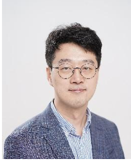
[Seminar] "Solution Processing of High-Performance Inorganic and Hybrid Materials for Large Area Electronics" by Prof. Myung-Gil Kim
Date
Thursday, September 3, 2026 - 15:30 to 16:30
Location
L5DE13
Description
"Solution Processing of High-Performance Inorganic and Hybrid Materials for Large Area Electronics"
Speaker:
Myung-Gil Kim, Ph.D. [CV]
Professor
School of Advanced Materials Science & Engineering
Sungkyunkwan University, Suwon, Republic of Korea
Abstract:
Large-area electronics require advanced semiconducting materials to support emerging applications such as high-performance thin-film solar cells, ubiquitous healthcare sensor arrays, and edge-computing artificial skin. While metal chalcogenides, metal oxides, and hybrid materials hold significant promise, developing general strategies for producing high-quality, large-area semiconductor films from soluble precursors remains a key focus of ongoing research.
This seminar presents recent advancements in high-performance solution-processed metal oxides, metal chalcogenides, metal halides, and hybrid nanomaterials. For metal oxides, hybrid transparent conducting electrodes maintain a high electrical conductivity of up to 555 S cm-1 under a 1 mm bending radius for 1,000 cycles. Additionally, surface passivation using self-assembled monolayers (SAMs) or organic semiconductors ensures stable operation under severe electrical bias and proton radiation, while anion alloying stabilizes high-indium content oxide semiconductors without small cations like gallium or zinc.
For metal chalcogenides, optimized thin-film transistor (TFT) devices achieve a maximum field-effect mobility exceeding 300 cm2 V-1 s-1, an on/off current ratio greater than 107, and a threshold voltage shift under 0.5 V during a 10 ks positive gate-bias stress. Furthermore, metal-chalcogenide-based seven-stage ring oscillators demonstrate an operating speed of approximately 2.6 MHz with a propagation delay under 27 ns per stage.
Moreover, recent developments in Zr-oxo cluster-based memristors deliver stable performance under mechanical bending, exhibiting an endurance of about 104 cycles, memory retention up to 104 seconds, and an Ion/Ioff ratio of 104 at a 2.5 mm bending radius. Featuring highly symmetric analog switching with multilevel conductance states, these devices achieve a pattern recognition accuracy of 97.44%, paving the way for high-precision neuromorphic computing.
Finally, we have developed transparent p-type electronics with CuI for p-type thin-film transistor (TFT) and p-type transparent conducting electrode (TCE). Initially, with the mild processing of CuI thin-film, we achieved successful control of iodine vacancy and decent TFT performance. As a continuous effort, the hole concentration suppression with Zn or Cd doping of CuI resulted high performance transparent TFT with hole mobility over 5 cm2 V-1 s-1, high Ion/Ioff of 107, high electrical bias stability, and circuit level integration with standar lithography compatibility. For p-type TCE, the S doping of CuI was achieved with liquid iodination process. The heavily S-doped CuI with unique liquid iodination and solution-process resulted large hole concentration of 3.25 × 1020 cm-3 and high conductivity of 511 S cm-1 with optical transmittance over 80 % at 550 nm. With the continuous development of materials and processing methods, the CuI could provide alternative solutions for high performance transparent p-type electronics.
All-OIST Category:
Subscribe to the OIST Calendar: Right-click to download, then open in your calendar application.