

FY2018 Annual Report
Femtosecond Spectroscopy Unit
Associate Professor Keshav Dani
Abstract
In recent years, the ability to synthesize, engineer & observe low dimensional materials, with properties determined by variations on the nanometer length scale has led to novel phenomena and applications. On the other hand, modern lasers deliver powerful, ultrashort pulses of light allowing us to observe the interaction of electrons and atoms on the femtosecond timescale. Together, these technologies allow us to study new paradigms in light-matter interaction – with femtosecond temporal resolution and nanometer spatial resolution. In FY2018, Femtosecond Spectroscopy Unit has directed these broad capabilities towards three different areas of study:
(a) Low-Dimensional Materials and Surface Dynamics, where we search for new functionality in materials with applications in optics, electronics and energy;
(b) Terahertz Devices & Applications, where we investigate the generation of broadband THz radiation and applying this to a variety of materials and devices;
(c) Quantum and Topological Materials, where we study and search for new phenomena at ultrafast timescales in correlated and topological materials.
1. Staff
- Dr. Keshav M. Dani, Professor
- Dr. Michael K. L. Man, Researcher
- Dr. Bala Murali Krishna, Researcher
- Dr. Julien Madéo, Researcher
- Dr. Christopher E. Petoukhoff, Researcher
- E Laine Wong, Graduate Student
- Viktoras Lisicovas, Graduate Student
- Andrew J. Winchester, Graduate Student
- Vivek Pareek, Graduate Student
- Joel Pérez Urquizo, Graduate Student
- Sofiia (Sonya) Kosar, Graduate Student
- Chakradhar Sahoo, Special Research Student
- Yumi Ito, Administrative Assistant
2. Collaborations
Theme: Low-Dimensional Materials and Surface Dynamics
- Type of collaboration: Joint research
- Researchers:
- A. Margiolakis, Department of Physics, Univ. of Crete, Greece
- G. D. Tsibidis, Department of Physics, Univ. of Crete, Greece
- G. P. Tsironis, Department of Physics, Univ. of Crete, Greece
Theme: Terahertz Devices and Applications
- Type of collaboration: Joint research
- Researchers:
- S. Vinod, Dept. of Materials Sci. & Nanoeng., Rice Univ., USA
- C. Tiwary, Dept. of Materials Sci. & Nanoeng., Rice Univ., USA
- P. M. Ajayan, Dept. of Materials Sci. & Nanoeng., Rice Univ., USA
Theme: Quantum and Topological Materials
- Type of collaboration: Joint research
- Researchers:
- C.P. Weber, Santa Clara University, USA
- M. G. Masten, Santa Clara University, USA
- T. C. Ogloza, Santa Clara University, USA
- B. Berggren, Santa Clara University, USA
- J. Liu, Tulane University, USA
- Z. Mao, Tulane University, USA
- D.D. Klug, National Res. Council, Ottawa, Canada
- A. A. Adelelke, Univ. of Saskatchewan, Canada
- Y. Yao, Univ. of Saskatchewan, Canada
- L. M. Schoop, Princeton Univ., USA
- S. Parkin, Max Planck Inst. Of Microstructure Physics, Germany
- R. Newby, Santa Clara Univ., USA
- A. Nateprov, Inst. Of Applied Physics, Moldova
- B. Lotsch, Ludwig-Maximilians-Universitat, Germany
- J. Kim, Santa Clara Univ., USA
- H. Bechtel, LBNL, California, USA
- E. Arushanov, Inst. Of Applied Physics, Moldova
- M. Ali, Max Planck Inst. Of Microstructure Physics, Germany
3. Activities and Findings
3.1 Low-Dimensional Materials and Surface Dynamics
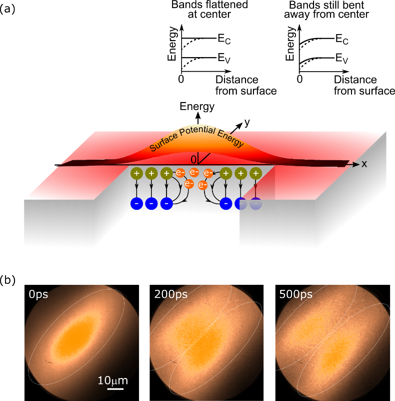
A. Pulling apart photoexcited electrons by photoinducing an in-plane surface electric field
[Science Advances 4, eaat9722 (2018)]
The ability to control the spatial and temporal dynamics of photoexcited charge carriers has played a central role in the development of modern optoelectronic technologies such as solar cells and photodetectors. At the heart of these technologies is the separation of oppositely charged photoexcited electron-hole pairs via the use of either an external electric field or the potential gradient across a semiconductor heterojunction. Going beyond, the ability to manipulate the spatiotemporal dynamics of similarly charged photoexcited electrons at ultrafast time scales could lead to novel optoelectronic technologies. In this study, we showed that by leveraging the spatial intensity variation within an ultrafast light pulse, we can manipulate the surface potential of a homogeneous semiconductor using the surface photovoltage effect. The induced surface field due to the spatially varying surface potential then allows us to pull apart the photoexcited electrons into two separate distributions (Fig. 1). We further demonstrated that the separation process can be controlled via the spatial profile and the intensity of the ultrafast light pulse.
B. Ultrafast dynamics and subwavelength periodic structure formation following irradiation of GaAs with femtosecond laser pulses
[Physical Review B 98, 224103 (2018)]
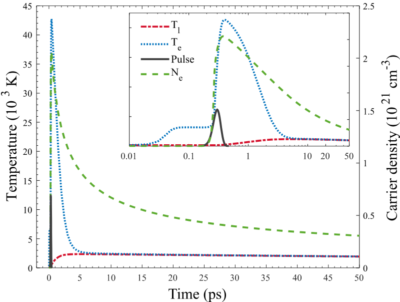
We performed a theoretical study of GaAs under femtosecond pulse laser irradiation, examined the ultrafast processes and dynamics of the excited carriers under conditions where the material was damaged, followed by surface modification of the heated solid (Fig.2). Different pulse duration values were compared to the produced transient carrier density in order to correlate them, for a parametric study under femtosecond laser irradiation, considering the fundamental multiscale physical processes.
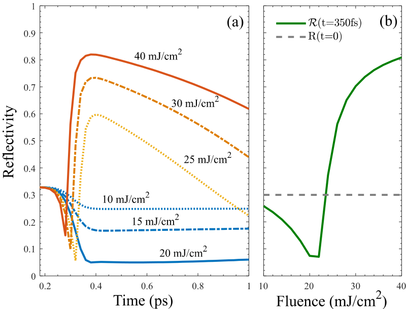
Even though the material is originally a semiconductor, under high fluence it displays a metallic behavior which is studied under a range of fluence (Fig. 3). Surface-plasmon waves are excited if a sufficient number of electrons in the conduction band are generated [1]. It is presented that when the surface plasmons couple with the laser incident waves and a fluid-based surface modification [1], it leads to subwavelength periodic structures with perpendicular direction in relation to the laser electric field polarization. The wavelength of the induced periodic structures and the damage threshold in experimental results are in good agreement with the theoretical predictions.
References Section 3.1 B:
[1] T. J. Y. Derrien, et al., Appl. Phys. A 117, 77 (2014).
[2] G. D. Tsibidis, et al., Phys. Rev. B 86, 115316 (2012).
3.2 Terahertz Devices and Applications
A. Terahertz photoconductivity and photocarrier dynamics in few-layer hBN/WS2 van der Waals heterostructure laminates
[Semicond. Sci. Technol. 33, 084001 (2018)]
Van der Waals heterostructures [1] is an emerging field of Nanoscience and Nanotechnology focusing towards on-demand properties for optoelectronic devices. Different two dimensional materials can be assembled into artificial structures to enable novel features and properties which are originating due to interlayer interactions [2,3]. Liquid phase exfoliation is allowing to fabricate designed artificial structures from nanoscale heterostructures to microscale laminates for novel device attributes [3]. We have fabricated self-assembled semiconducting WS2 and WS2 with insulating hBN laminates for the study of photocarrier dynamics and photoconductivity. The photocarrier dynamics were measured through optical pump-terahertz probe (OPTP) technique. An unusual OPTP signal was obtained for WS2/hBN which is raise in negative differential signal as illustrated in the Fig. 4a. The understanding of this unusual response obtained by fitting curves of the Fig. 4a through modelling via rate equations which involve different carriers such as electrons, holes, excitons and interface dipoles. The density of carriers obtained for best fits were plotted in the Fig. 4b.
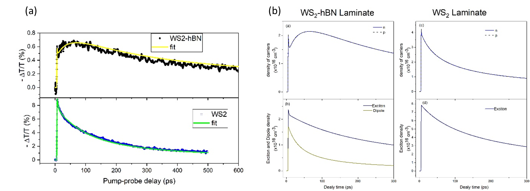
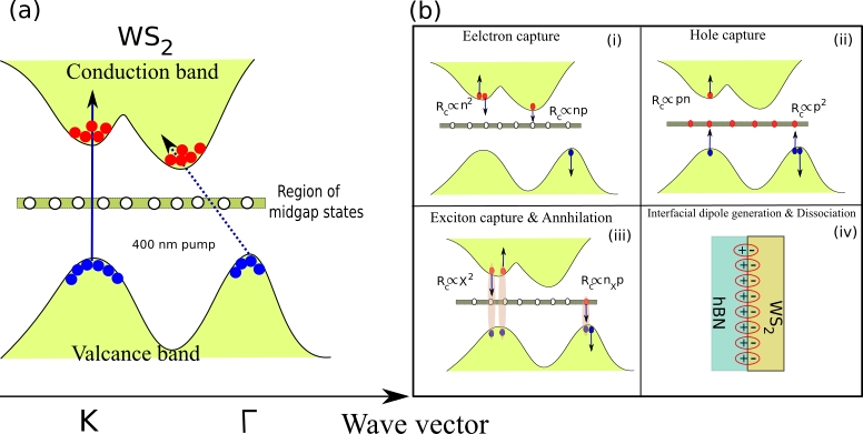
Due to the disorder layer staking in the laminates, they have various kind of defects including vacancies, structural defects, folding, wrinkling and passivation of edges, grain boundaries. Some of these defects create mid-gap states/trap states in the laminates, which are intern act as a recombination centers for carriers. Upon photoexcitation, carriers are created and recombined via different recombination procedures including trap assisted as shown in the Fig. 5. Our model is consistent with reported literature [4] and drawn useful information regarding photocarriers and interfacial dipoles.
Further, the formation of interfacial dipoles in WS2/hBN laminate also confirmed by the frequency dependent photoconductivity studies. These type of materials are useful in developing the new kind of THz devices such as phase shifter and modulators.
References Section 3.2 A:
[1] A. K. Geim, et al., Nature 499, 419 (2013).
[2] H. Fang, et al., Proc. Nat. Acad. Sci. 111, 6198 (2014).
[3] M. B. M. Krishna, et al., Adv. Opt. Mater. 3, 1551 (2015).
[4] J. H. Strait, et al., Phys. Rev. B 90, 245402 (2014).
3.3 Quantum and Topological Materials
A. Using coherent phonons for ultrafast control of the Dirac node of SrMnSb2
[Phys. Rev. B 98, 155115 (2018)]
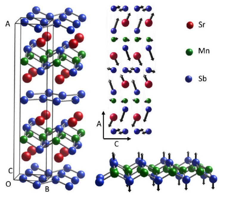
SrMnSb2 is a candidate Dirac semimetal whose electrons near the Y point have the linear dispersion and low mass of a Dirac cone[1,2]. Through first-principles calculations of the electronic and phononic structure of SrMnSb2, we showed that it is possible to use coherent phonon oscillation to periodically open and close a gap in the Y-point Dirac node of SrMnSb2 and we have identified the vibrational mode responsible, an Ag photon mode, named mode 36 as illustrated in Fig. 6, at 4.4 THz. Experimentally, we have shown that coherent oscillations of mode 36 in Sr0.94Mn0.92Sb2 are readily excited by ultrafast, 800nm optical pulses. The use of coherent phonons to control SrMnSb2 thus benefits from a solid experimental foundation. It would allow sub picosecond, on-and-off control of the Dirac node independently of photoexcited carriers and could lead to new opportunities to study and manipulate 3D Dirac electrons.
References Section 3.3 A:
[1] M. A. Farhan, et al., J. Phys: Condens. Matter 26, 042201 (2014).
[2] S. V. Ramankutty, et al., SciPost Phys. 4, 010 (2018).
B. Directly photoexcited Dirac and Weyl fermions in ZrSiS and NbAs
[Applied Physics Letters 113, 221906 (2018)]
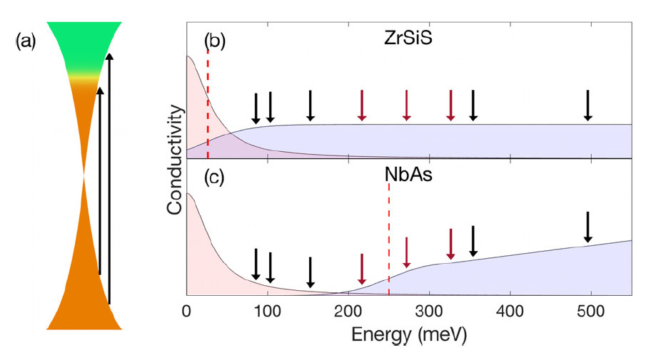
Recently, there are wide interest in topological semimetals whose low-energy excitation are Dirac or Weyl fermions [1-3]. Here, we report ultrafast optical measurements of the Dirac line-node semimetal ZrSiS and the Weyl semimetal NbAs, using mid-infrared pump photons from 86meV to 500meV to directly excite Dirac and Weyl fermions within the linearly dispersing bands. Fig. 7 illustrates the scheme of the measurements. In NbAs, the photoexcited Weyl fermions initially form a non-thermal distribution, signified by a brief spike in the differential reflectivity whose sign is controlled by the relative energy of the pump and probe photons. In ZrSiS, electron-electron scattering rapidly thermalizes the electrons, and the spike is not observed. Subsequently, in both materials hot carriers are cooled within a few picoseconds. This cooling, as seen in the two materials’ differential reflectivity, differs in sign, shape, and timescale. Nonetheless, we find that this cooling of hot carriers may be described in a simple model of thermal electrons, without free parameters. The electronic cooling in ZrSiS is particularly fast, our result suggests that ZrSiS, in addition to being non-toxic and earth abundant, may support faster optical switches and detectors than Cd3As2 does.
References Section 3.3 B:
[1] A. A. Burkov, et al., Phys. Rev. B 84, 235126 (2011).
[2] S. M. Young, et al., Phys. Rev. Lett. 108, 140405 (2012).
[3] H. Weng, et al., Phys. Rev. X 5, 011029 (2015).
4. Publications
4.1 Journals
- A. Margiolakis, G. D. Tsibidis, K. M. Dani, and G. P. Tsironis, Ultrafast dynamics and subwavelength periodic structure formation following irradiation of GaAs with femtosecond laser pulses, Phys. Rev. B 98, 224103 (2018).
- C. P. Weber, L. M. Schoop, S. S. P. Parkin, R. C. Newby, A. Nateprov, B. Lotsch, B. M. K. Mariserla, J. M. Kim, K. M. Dani, H. A. Bechtel, E. Arushanov, and M. Ali, Directly photoexcited Dirac and Weyl fermions in ZrSiS and NbAs, Appl. Phys. Lett. 113, 221906 (2018).
- C. P. Weber, M. G. Masten, T. C. Ogloza, B. S. Berggren, M. K. L. Man, K. M. Dani, J. Liu, Z. Mao, D. D. Klug, A. A. Adeleke, and Y. Yao, Using coherent phonons for ultrafast control of the Dirac node of SrMnSb2, Phys. Rev. B 98, 155115 (2018).
- E L. Wong, A. J. Winchester, V. Pareek, J. Madéo, M. K. L. Man, and K. M. Dani, Pulling apart photoexcited electrons by photoinducing an in-plane surface electric field, Science Advances 4, eaat9722 (2018).
- M. B. M. Krishna, J. Madéo, J. P. Urquizo, X. Zhu, S. Vinod, C. S. Tiwary, P. M. Ajayan, and K. M. Dani, Terahertz photoconductivity and photocarrier dynamics in few-layer hBN/WS2 van der Waals heterostructure laminates, Semicond. Sci. Tech. 33, 084001 (2018).
4.2 Books and Other One-Time Publications
Nothing to report.
4.3 Oral and Poster Presentations
- Winchester, A. J., Petoukhoff, C. E., Abdi-Jalebi, M., Andaiji-Garmaroudi, Z., Pareek, V., Wong, E., Madeo, J., Man, M. K. L., Stranks, S. D., Dani, K. M., Investigation of Trap States and Their Dynamics in Hybrid Organic-inorganic Mixed Cation Perovskite Films Using Time Resolved Photoemission Electron Microscopy, Oral Presentation, CLEO2018, San Jose, CA, USA May 15-17 (2018)
- Wong, E., Winchester A. J., Man, M. K. L., Pareek, V., Madeo, J., Dani, K. M., Ultrafast separation of photoexcited electron cloud, Oral Presentation, CLEO2018, San Jose, CA, USA May 15-17 (2018)
- Petoukhoff, C. E., Voiry, D., Bozkurt, I., Chhowalla, M., Dani, K. M., Probing Charge Transfer States in Polymer: Fullerene – MoS2 van der Waals Heterostructures, Oral Presentation, CLEO2018, San Jose, CA, USA May 15-17 (2018)
- Wong, E., Winchester A. J., Man, M. K. L., Pareek, V., Madeo, J., Man, M. K. L., Dani, K. M., Manipulating the distribution of photoexcited electrons on ultrafast timescales, Oral Presentation, UP2018, Hamburg, Germany Jul 15-20 (2018)
- Petoukhoff, C. E., Kosar, S., Dani, K. M., Photoinduced Charge Transfer Dynamics in Organic- MoS2 Mixed-Dimensional van der Waals Heterojunctions, Invited Talk, PIERS, Toyama, Japan Aug 1-4 (2018)
- Man, M. K. L, HHG based time resolved photoemission spectroscopy and microscopy, Poster Presentation, LEEMPEEM11, Chongqing, China, Oct 30 - Nov 3 (2018)
- Winchester, A. J., Petoukhoff, C. E., Macpherson, S., Abdi-Jalebi, M., Andaji-Garmaroudi, Z., Pareek, V., Wong, E., Madeo, J., Man, M. K. L., Stranks, S. D., Dani, K. M., Imaging the ultrafast phot-hole trapping at nanoscale defect sites in perovskite photovoltaic films, Oral Presentation, LEEMPEEM11, Chongqing, China, Oct 30 - Nov 3 (2018)
- Wong, E., Winchester, A. J., Pareek, V., Madeo, J., Man M. K. L., Dani, K. M., Pulling apart photoexcited electron cloud, Oral Presentation, LEEMPEEM11, Chongqing, China, Oct 30 - Nov 3 (2018)
- Winchester, A. J., Petoukhoff, C. E., Macpherson, S., Abdi-Jalebi, M., Andaji-Garmaroudi, Z., Pareek, V., Wong, E., Madeo, J., Man, M. K. L., Stranks, S. D., Dani, K. M., Imaging the ultrafast phot-hole trapping at nanoscale defect sites in perovskite photovoltaic films, Oral Presentation, MRS2018 Fall, Boston, MA, USA, Nov 25-30 (2018)
- Urquizo, J. P., Madeo, J., Todorov, Y., Li, L., Davies, A. G., Linfield, E., Sirtori, C., Dani K. M., Controlling the losses and beam shape in arrays of THz patch antenna microcavities, Poster Presentation, The 3rd Photonics Workshop, Okinawa, Japan, Nov 30- Dec 1 (2018)
- Dani, K. M., Time Resolved Photoemission Electron Microscopy of Semiconductors, Invited Talk, The 3rd Photonics Workshop, Okinawa, Japan, Nov 30- Dec 1 (2018)
- Dani, K. M., Exploring Spatial Variations in Ultrafast Photocarrier Dynamics in Semiconductors Structures, Invited Talk, EPIC2018, Singapore, Dec 5-7 (2018)
- Urquizo, J. P., Madeo, J., Todorov, Y., Li, L., Davies, A. G., Linfield, E., Sirtori, C., Dani K. M., Patch antenna microcavities for THz Emission, Poster Presentation, Optical Terahertz Science and Technology Conference2019, Santa Fe, NM, USA, Mar 10-15 (2019)
5. Intellectual Property Rights and Other Specific Achievements
Nothing to report.
6. Meetings and Events
6.1 Seminar
- Date: Apr 10th 2018
- Venue: C700, OIST Campus
- Speaker: Dr. Ashwani Sastry
- Date: July 5th 2018
- Venue: C209 OIST Campus
- Speaker: Dr. Xiaoqin Elaine Li
- Date: July 24th 2018
- Venue: C210 OIST Campus
- Speaker: Dr. Samuel D. Stranks
- Date: Aug 8th 2018
- Venue: B503 OIST Campus
- Speaker: Dr. Motoaki Bamba
- Date: Aug 27th 2018
- Venue: C209, OIST Campus
- Speaker: Dr. Mack Kira
- Date: Sep 18th 2018
- Venue: C700 OIST Campus
- Speaker: Dr. Richarj Mondal
- Date: Oct 23rd 2018
- Venue: C210 OIST Campus
- Speaker: Pauline Uring
- Date: Nov 27th 2018
- Venue: B503 OIST Campus
- Speaker: Dr. Robert Riedel
- Date: Dec 14th 2018
- Venue: C016 OIST Campus
- Speaker: Dr. Alexander Gliserin
6.2 Workshop
Nothing to report.
7. Others
Nothing to report.