

FY2011 Annual Report
Energy Materials and Surface Sciences Unit
Abstract
Our Unit is making concerted effort to investigate relevant surfaces and interfaces with advanced experimental techniques such as scanning probe microscopy, photoemission spectroscopy, charge transport measurements, etc.
1. Staff
- Dr. Michael Lee, Group Leader
- Dr. Min-Cherl Jung, Researcher
- Dr. Haijun Fan, Researcher
- Alison Cross, Graduate Student (Exchange program)
- Taki Tazuke, Secretary
2. Collaborations
- Theme: Electronic structures of organic-based field effect transistor studied with synchrotron radiation
- Type of collaboration: Cowork
- Researchers:
- Beamline manager, Dr. Han-Koo Lee, Pohang Accelerator Laboratory
- Beamline manager, Dr. Hyun-Joon Shin, Pohang Accelerator Laboratory
3. Activities and Findings
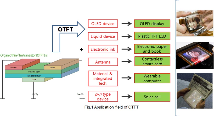
3.1 Organic-based thin-film transistor (OTFT)
The fabrication and characterization of ultra-thin (~ 6 nm) film for OTFT devices [Dr. Jung]
- Development and characterization of the prostrate and upright TIPS-Pentacene layers with high electrical mobility for organic thin-film transistors
Recently, the research field of organic thin-film transistor (OTFT) is dramatically expanding for many applications. OTFT devices can have three important advantages over traditional inorganic devices: 1) flexible substrate, 2) very low cost, and 3) simple processing. These advantages open the field to applications that have been closed to products based on traditional technology (Fig.1) Some examples are light-weight rollable or foldable screens, wearable electronics, or electronic paper. These applications depend strongly on the successful design and production of electronic devices based on OTFT. One especially important property for the organic films on which OTFTs depend is the carrier mobility. The deposition conditions need to be carefully controlled to obtain high carrier mobility in the organics.
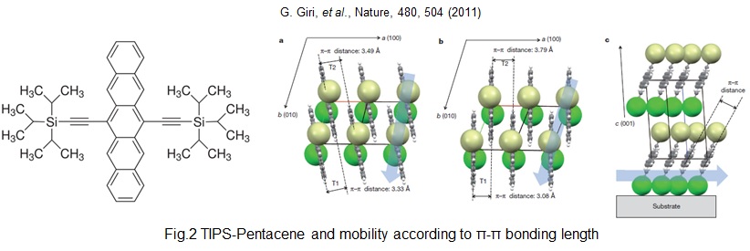
For the enhancement of high mobility in organics, we need to study: ① crystallization by heating the substrate to promote self-assembly without impurities, ② molecular design with the easy intermolecular conduction, and ③ doping effect without sacrificing conductivity. In this respect, 6,13-bis(triisopropylsilylethynyl) (TIPS)-Pentacene (Fig. 2) is a very interesting organic semiconductor because it shows high mobility (1.8 ~ 5 cm2/V·s), is stable in air, and is amenable to easy fabrication methods like spin-coating and inkjet-printing that don't require vacuum. Also, many researchers have reported on the deposition and properties of TIPS-Pentacene. The high mobility of TIPS-Pentacene is due to the vertical alignment of molecules on the surface, which increases π-π bondings. However, most fabrication methods are not compatible with the current Si-based industry, which requires significantly more infrastructure than the systems for the deposition of TIPS-Pentacene. In general, the process steps required for Si-based device fabrication number over 300. Fabrication of Si-based transistor for example, requires 50 processes in detail. (litho→etch→depo→litho→etch→…) If we can find and optimize a fabrication method for well-defined TIPS-Pentacene with high mobility, we can shorten the process by using only a spin-coater.
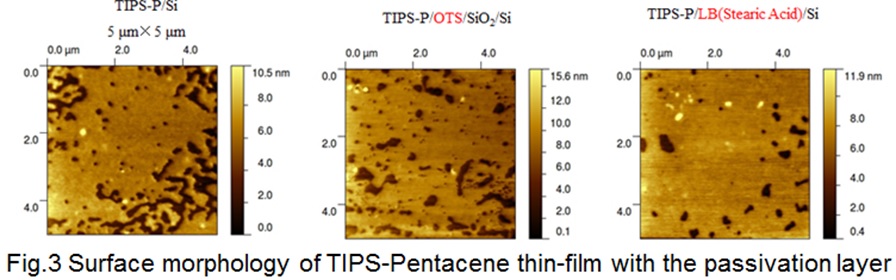
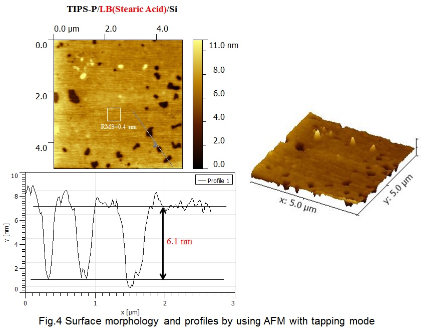
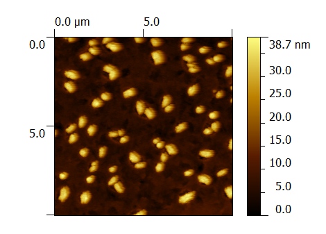
In our preliminary experiments, we can control the of a TIPS-Pentacene thin film on a Si wafer to be 2.5 ~ 3.0 nm. (Fig. 3 and 4) When a passivation layer is used first, we find a more complete coverage (> 80%). This demonstrates the possibility of thickness and flatness control by using the spin-coater. Additionally we performed small-angle x-ray scattering to measure the crystallinity of the TIPS-Pentacene surface. In Fig 5., we can observe the highly crystalline nature of the TIPS-Pentacene surface.
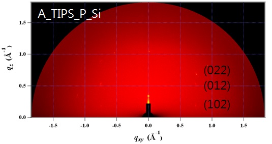
Figure 5. Small-Angle X-ray Scattering of a TIPS-Pentacene film that is only a few nanometers thick.
Angle-resolved NEXAFS and XPS analysis with synchrotron radiation at Pohang Accelerator Laboratory in the Republic of Korea, measure the chemical states of a TIPS-Pentacene/Si sample, as shown in Fig. 6. In all results, we will make and characterize the prototype OTFT device.
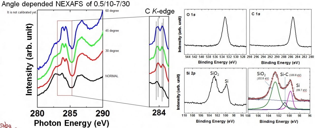
Figure 6. Angle-resolved NEXASFS (left) and XPS (right) of a TIPS-Pentacene film that is only a few nanometers thick. The different NEXAFS curves represent spectra obtained at different incident angles of irradiation. The XPS spectra include O1s, C1s, and Si2p spectra. Fitting the Si2p spectrum revealed three different peaks, from silicon dioxide, silicon crystal, and Si-C bonds.
3.2 Organic-based photovoltaic device (OPD)
The optimization of photovoltaic device performance [Dr. Fan]
This research interest mainly involves optimization of photovoltaic device performance, and further understanding of the physical processes involved in organic photovoltaics, especially those processes occurring at the surface and interfaces. Herbert Kroemer, a Nobel laureate, summarized the observations of many researchers on electronic processes with the famous phrase “the interface is the device”. Realizing its importance, we also focus on the interfaces in solar devices. Recently we have been doing research work on introducing novel interface modification layers into organic electronic devices by using a simple, method with precise control over the thickness of monolayers, namely the Langmuir-Blodgett film method. Compression curves are shown below in Fig. 7 and AFM images of the resulting films are shown in Fig. 8. We investigate the effect of organic (or inorganic) modification layers in devices. We have prepared fine thin transparent films on different substrates, like glass, Silicon wafer, and ITO, by using different amphiphilic organic molecules, and study the surface morphology, electrical properties, and optical properties of these films. Meanwhile, we are trying to make organic photoelectric devices improve the efficiency of organic based solar cells.
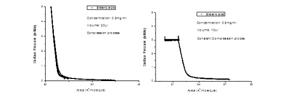
Fig 7. Typical curves for LB film forming process(left: Compression process; right Constant compression process)
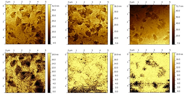
Fig 2. AFM height images (top) and current images (bottom). From left to right: 1 layer, 3 layers, 5 layers deposited by the Langmuir-Blodgett method.
Improvement and finding of the optimum processing parameters [Ms. Cross]
This work focuses on improving the efficiency of organic solar cells. I will use organic materials which are much cheaper than the materials currently used in state-of-the-art solar cells. The techniques available within our group for fabricating the devices also place an emphasis on low cost, for example solution-based techniques that are fast and do not require high vacuum or high temperatures. The approach to increasing solar cell efficiency will be two-fold: 1) investigating the optimum processing parameters and 2) exploring novel device configurations. The success of these strategies will be evaluated using a range of characterization techniques including atomic force microscopy, XPS/UPS (X-ray and Ultraviolet photoelectron spectroscopy) and a solar cell testing station.
4. Publications
4.1 Journals
Yabing Qi, “Investigations of organic films by atomic force microscopy: structural, nanotribological and electrical properties”, Surface Science Reports 66, 379 (2011). (Invited review)
4.2 Books and other one-time publications
Nothing to report
4.3 Oral and Poster Presentations
-
Yabing Qi, “Unusual conductivity enhancement on oligothiophene Langmuir-Blodgett monolayers studied by current-sensing AFM”, 10th International Symposium on Functional π-Electron Systems, Beijing, China (October 13-17, 2011). (Poster presentation)
-
Yabing Qi, “Investigation of organic films by spectroscopy, charge transport measurements and microscopy”, Institute of Physics, Chinese Acamemy of Science, Beijing, China (October 19, 2011). (Invited oral presentation)
-
Yabing Qi, “Investigation of organic films by spectroscopy, charge transport measurements and microscopy”, Peking University, Beijing, China (October 20, 2011). (Invited oral presentation)
-
Yabing Qi, “Electronic properties of organic films”, 1st Annual World Congress of Nano-S&T, Dalian, China (October 23-26, 2011). (Invited oral presentation)
-
Yabing Qi et al., “Electrical Properties of Organic Semiconductors n-Doped with Air-Stable Dopants”, Materials Research Society Fall Meeting, Boston, Massachusetts (November 28-December 2, 2011) (Poster presentation)
-
Yabing Qi, “Environment, Energy and You”, Yamada Junior High School (December 8, 2011). (Oral presentation)
-
Yabing Qi, “Investigating organic / hybrid solar cells with a surface science approach”, Okinawa Industry-Academia-Government Collaboration Innovation Forum FY2011 (Okinawa Innovation Forum 2011) (December 16, 2011). (Oral presentation)
-
Yabing Qi, “Clean energy future: battle against global warming”, Open Campus 2012: Experience the World of Science (March 18, 2012). (Oral presentation)
-
Yabing Qi et al., “Morphology control of organic semiconductor films via surface modification”, 2nd International Workshop-Toward the development of an R&D Cluster in Okinawa (March 30, 2011). (Poster presentation)
5. Intellectual Property Rights and Other Specific Achievements
Nothing to report
6. Meetings and Events
6.1 Seminar
- Date: August 30, 2011
- Venue: OIST Campus Lab1
- Speaker: Prof. Weijia Wen (Department of Physics, The Hong Kong University of Science and Technology).
- Date: November 7, 2011
- Venue: OIST Campus Lab1
- Speaker: Prof. Jeong Young Park (Graduate School of EEWS and NanoCentury KI, KAIST (Korea Advanced Institute of Science and Technology).Date: March 10, 2012
- Date: December 15, 2011
- Venue: OIST Campus Lab1
- Speaker: Dr. Jian Ting Ye (Quantum-Phase Electronics Center, Department of Applied Physics, The University of Tokyo).Date: March 10, 2012
- Date: March 10, 2012
- Venue: OIST Campus Lab1
- Speaker: Dr. Kato (Institute of Engineering Innovation, The University of Tokyo).
- Date: April 16, 2012
- Venue: OIST Campus Lab1
- Speaker: Christina Chiutu (Nanoscience Group, School of Physics and Astronomy, University of Nottingham, United Kingdom).
- Date: April 20, 2012
- Venue: OIST Campus Lab1
- Speaker: Adam Sweetman (School of Physics, University of Nottingham, Kings College London Strand, London).
- Date: May 21, 2012
- Venue: OIST Campus Lab1
- Speaker: Yuichi Kato (Graduate School of Engineering, Kyushu University, Fukuoka, Japan).
- Date: June 15, 2011
- Venue: OIST Campus Lab1
- Speaker: Prof. Liang-Yao Chen (Department of Optical Science and Engineering, Fudan University, China).
7. Other
Nothing to report.