

“Accelerating Particles into Space and Medicine" Profs. Kumada, Yoshioka, Takahashi, Arai and Sugawara

Date
Location
Description
Programme
Part I: Introduction to OIST BNCT
Speakers: Prof. Hiroaki KUMADA (Associate Professor, Medical Physicist, University of Tsukuba), Prof. Masakazu YOSHIOKA (Professor Emeritus, KEK; Visiting Professor, OIST, Tohoku University and Iwate University; Visiting Researcher, University of Tsukuba)
Part II: Introduction to New Technology for X-ray and Gamma-ray Imaging
Speakers: Prof. Tadayuki TAKAHASHI (Professor, Institute of Space and Astronautical Science (ISAS), JAXA, Department of Physics, University of Tokyo, High Energy Astrophysics), Prof. Yasuo Arai (Professor, KEK, Institute of Particle and Nuclear Studies, Electronics System Group; Visiting Professor, OIST)
Closing: Our Future - Beyond Metastasis
Remarks by Prof. Hirotaka Sugawara (Distinguished Professor, OIST)
Abstracts
Part I: "Introduction to OIST BNCT" by Profs. Yoshioka and Kumada
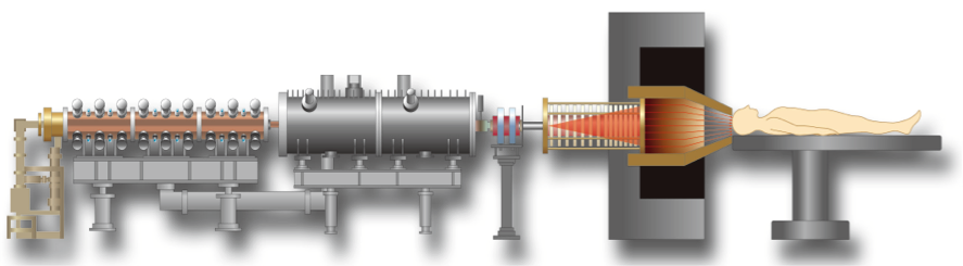
An accelerator-based BNCT (Boron Neutron Capture Therapy) facility is being constructed and tested at the Ibaraki Neutron Medical Research Center (INMRC). It consists of a proton linac (8 MeV energy and 10mA average current), a beryllium target, and a moderator system to provide an epi-thermal neutron flux for patient treatment. The technology choices for this present system were driven by the need to site the facility in a conventional hospital setting and where low residual radioactivity would be essential. The maximum neutron energy produced from an 8 MeV-proton is 6 MeV, which is below the threshold energy of the main nuclear reactions that result in radioactive products. The down side of this technology choice is that it produces a high-density heat load on the target; therefore efficient cooling and amelioration of hydrogen blistering present sever challenges to the R&D, finding successful solutions would be crucial. The latest design of the target and moderator system shows that a flux of 4.7×10⁹ epi-thermal neutrons / cm2 / sec can be obtained.
Based on the above results and experiences, it has become clear that a mass production model of a BNCT facility could be simplified more and more with a reduction in the system size and cost by adopting following technologies. The OIST BNCT facility should be the first mass production model of the accelerator-based BNCT facility.
- One single beam klystron (SBK) as used at INMRC could be replaced with two or three multi-beam klystrons (MBK). The MBK is now well established through the R&D for the ILC. By using an MBK, the necessary high-voltage for the klystron modulator can be lowered from -90kV to -30~-50kV, which will give very big impacts to the cost, availability and operability.
- The RF frequency of the INMRC linac is 324MHz, which is slightly lower than the optimum RF frequency for the BNCT.
- The beam transport design for the INMRC facility is not optimum one for the BNCT, because its building is not newly constructed but remodeled from the existing building.
- We have found many issues to be improved through the beam commissioning of the INMRC facility.
We will report the current status of the INMRC facility and the baseline design of the OIST-BNCT.
Part II: Introduction to New Technology for X-ray and Gamma-ray Imaging
(1) Presentation by Prof. Tadayuki Takahashi (ISAS, JAXA) (30 min.)
The good energy resolution and the ability to fabricate compact arrays make semiconductor sensors very attractive for the imaging application in comparison with inorganic scintillation detectors coupled to either photodiodes or photomultiplier tubes. Though Si and Ge semi- conductors have been widely used, still, there are increasing demands for new semiconductor detectors capable of detecting hard X-ray and Gamma-rays. Cadmium telluride (CdTe) has been regarded as promising semiconductor materials for hard X-ray and gamma-ray detection, which can be operated at room temperature. Especially a large-area CdTe imaging detector with an area greater than a few tens of square centimeters with energy resolution of 1 to 2 keV (FWHM) is attractive for various applications.
The hard X-ray and gamma-ray bands have long been recognized as important windows for exploring the energetic universe. It is in these energy bands that non-thermal emission, primarily due to accelerated high-energy particles, becomes dominant. However, when compared with X-ray astronomy, hard X-ray and gamma-ray astronomy are still immature. In order to realize instruments providing much improved angular and spectral resolutions over the instruments in use today, we have been working on various types of CdTe detectors based on technologies such as electrodes on the device, ASICs for readout and hybridization for making large-scale detectors.
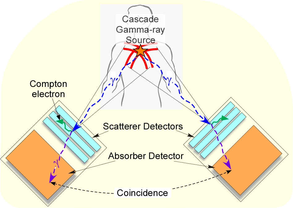
After 10 years of research and development, CdTe diode detectors have now entered the phase of actual application. In particular, the fine energy and position resolution obtained with CdTe pixel detectors or CdTe DSDs (Double Sided Detectors) are expected to lead to dramatically improved performance in the area of gamma-ray imaging. For astronomical observations, developments of Hard X-ray Imager (HXI) and Soft Gamma-ray Detector (SGD) based on the CdTe diode detectors are being progressed satisfactorily for the Japanese ASTRO-H satellite. HXI utilizes the large area CdTe DSD on the focal plane of the hard X-ray mirror while SGD is composed of 40-layer Si/CdTe Compton cameras. The direction of the gamma-ray is calculated by solving the Compton kinematics with information concerning deposit energies and interaction positions recorded in the detectors. A very compact, high-angular resolution (fineness of image) camera is realized by fabricating semiconductor imaging elements made of Si and CdTe, which have excellent performance in position resolution, high-energy resolution, and high-temporal resolution.


The technology developed here would also offer improved sensitivity in gamma-ray detection for various applications, including nuclear medical imaging, and nondestructive industrial imaging. In the field of medical imaging, a radiopharmaceutical, a pharmaceutical labeled by radioisotopes, injected into a living object need to be visualized. Although the potential performance of this kind of detector was proposed in early 1970s, adequate spatial resolution for medical use has not been achieved by traditional sensor technologies. It is only quite recently that semi-conductor based Compton Cameras has been made available. Since the CdTe imagers and the Si/CdTe semiconductor Compton camera have wide-band imaging capability from a few tens keV to MeV, various radioisotopes can be used. Moreover, simultaneous tracking of multiple radiopharmaceuticals could be realized by the capability to precisely distinguish emission lines from different radioisotopes.
Here we describe new technologies for X-ray and Gamma-ray imaging, which have been developed for highly sensitive detectors onboard high energy astronomy satellites. We also introduce our recent activities for future detectors, such as an electron-tracking Si/CdTe Compton camera.
(2) "Monolithic Radiation Image Sensor with Silicon-On-Insulator" by Prof. Yasuo Arai (30 min.)
Radiation image sensors using a Silicon-On-Insulator (SOI) technology have been developed at KEK. By using the SOI technology, thick sensing region and CMOS readout circuit are implemented in a single die. Special process to realize such detector has been developed in collaboration with a semiconductor company.
The SOI pixel detector (SOIPIX) can achieve high resolution and good sensitivity due to its fine lithography of semiconductor process. In addition, it can be very intelligent by including in-pixel data processing circuit such as counter, comparator, memory, ADC, TDC, and so on.
The detector can be sensitive to many kinds of radiations (X-ray, electron, alpha, charged particles, neutron etc.), so various kinds of detectors are being developed through Multi Project Wafer (MPW) runs operated by KEK. Now this R&D is operated under Grant-in-Aid for Scientific Research (KAKENHI) on Innovative Areas, and has more than 50 collaborators.
Recent results and present status will be presented.
Subscribe to the OIST Calendar: Right-click to download, then open in your calendar application.